M2V64S30DTP-7
M2V64S30DTP-7 is 64M Synchronous DRAM manufactured by Mitsubishi Electric.
DESCRIPTION
M 2V64S20DTP is a 4-bank x 4,194,304-word x 4-bit, M 2V64S30DTP is a 4-bank x 2,097,152-word x 8-bit, M 2V64S40DTP is a 4-bank x 1,048,576-word x 16-bit, synchronous DRAM , with LVTTL interface. All inputs and outputs are referenced to the rising edge of CLK. M 2V64S20DTP, M 2V64S30DTP and M 2V64S40DTP achieve very high speed data rate up to 133MHz for -6, and are suitable for main memory or graphic memory in puter systems.
Features
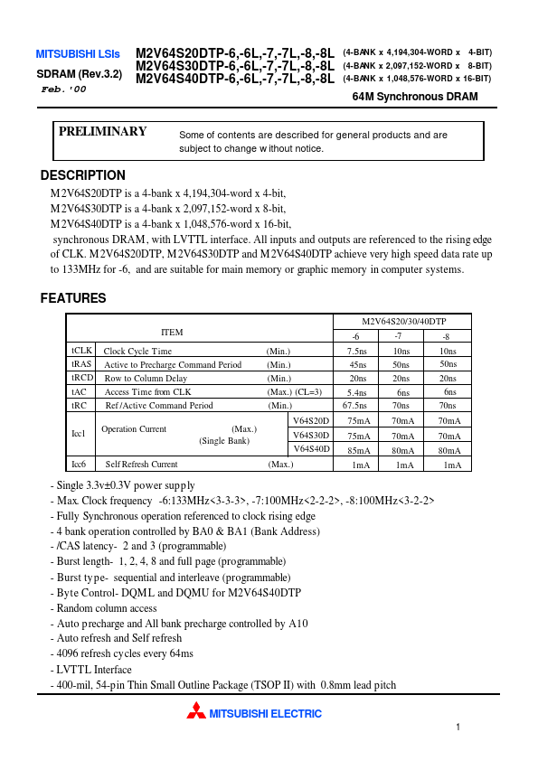
M2V64S20/30/40DTP ITEM t CLK t RAS t RCD t AC t RC Icc1 Clock Cycle T ime Active to Precharge mand Period Row to Column Delay Access Time from CLK Ref /Active mand Period Operation Current (Max.) (Single Bank) (Min.) (Min.) (Min.) (Max.) (CL=3) (Min.) V64S20D V64S30D V64S40D Icc6 Self Refresh Current (Max.) -6 7.5ns 45ns 20ns 5.4ns 67.5ns 75m A 75m A 85m A 1m A -7 10ns 50ns 20ns 6ns 70ns 70m A 70m A 80m A 1m A -8 10ns 50ns 20ns 6ns 70ns 70m A 70m A 80m A 1m A
- Single 3.3v±0.3V power supply
- Max. Clock frequency -6:133MHz<3-3-3>, -7:100MHz<2-2-2>, -8:100MHz<3-2-2>
- Fully Synchronous operation referenced to clock rising edge
- 4 bank operation controlled by BA0 & BA1 (Bank Address)
- /CAS latency- 2 and 3 (programmable)
- Burst length- 1, 2, 4, 8 and full page (programmable)
- Burst type- sequential and interleave (programmable)
- Byte Control- DQM L and DQMU for M2V64S40DTP
- Random column access
- Auto p recharge and All bank precharge controlled by A10
- Auto refresh and Self refresh
- 4096 refresh cycles every 64ms
- LVTTL Interface
- 400-mil, 54-pin Thin Small Outline Package (TSOP II) with 0.8mm lead pitch MITSUBISHI ELECTRIC
MITSUBISHI LSIs SDRAM (Rev.3.2) Feb.'00
M2V64S20DTP-6,-6L,-7,-7L,-8,-8L M2V64S30DTP-6,-6L,-7,-7L,-8,-8L M2V64S40DTP-6,-6L,-7,-7L,-8,-8L
(4-BANK x 4,194,304-WORD x (4-BANK x 2,097,152-WORD x
4-BIT) 8-BIT)
(4-BANK x 1,048,576-WORD x 16-BIT)
64M Synchronous DRAM
PIN CONFIGURATION (TOP VIEW) M2V64S20DTP M2V64S30DTP M2V64S40DTP
PIN CONFIGURATION (TOP VIEW)
Vdd NC Vdd Q NC DQ0 Vss Q NC NC Vdd Q NC DQ1 Vss Q NC...