Datasheet4U Logo Datasheet4U.com

M52693SP - BURST LOCK CLOCK GENERATOR

General Description

The M52693SP is a semiconductor integrated circuit developed for analog signal processing of a picture-in-picture system, consisting of a sync separator, an ACC, a burst lock clock generator circuit, an analog switch and a clamp circuit, etc.

Key Features

  • Low power dissipation of supply voltage 5.0V and circuit current 32mA (Typ. ) Built-in 4fsc burst lock clock generator circuit required for digital video signal processing Small picture chroma level following main picture burst level Main picture pedestal level matching small picture pedestal level Built-in reference voltage source for A/D converter ACC FILTER 10 VCXO IN 11 VCA CAP. 12 MAIN CHROMA IN 13 MAIN VIDEO OUT 14 SYNC SEP. IN 15.

📥 Download Datasheet

Full PDF Text Transcription (Reference)

The following content is an automatically extracted verbatim text from the original manufacturer datasheet and is provided for reference purposes only.

View original datasheet text
MITSUBISHI ICs (AV COMMON) M52693SP BURST LOCK CLOCK GENERATOR DESCRIPTION The M52693SP is a semiconductor integrated circuit developed for analog signal processing of a picture-in-picture system, consisting of a sync separator, an ACC, a burst lock clock generator circuit, an analog switch and a clamp circuit, etc. It is also available on digital video signal systems other than the above. 
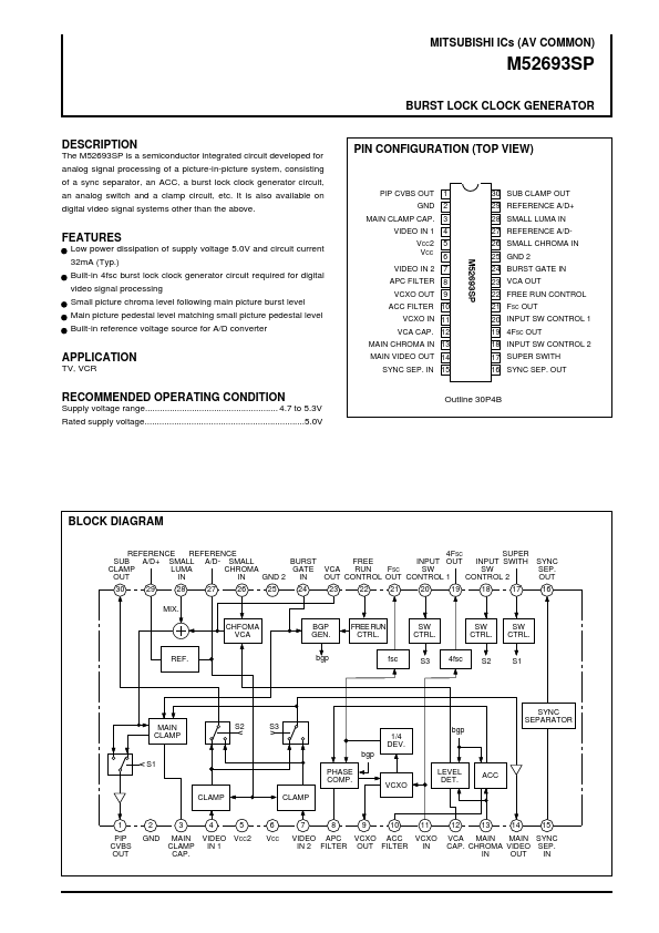
PIN CONFIGURATION (TOP VIEW) PIP CVBS OUT GND MAIN CLAMP CAP. VIDEO IN 1 VCC2 VCC VIDEO IN 2 APC FILTER VCXO OUT 1 2 3 4 5 6 7 8 9 30 SUB CLAMP OUT 29 REFERENCE A/D+ 28 SMALL LUMA IN 27 REFERENCE A/D26 SMALL CHROMA IN 25 GND 2 24 BURST GATE IN 23 VCA OUT 22 FREE RUN CONTROL 21 FSC OUT 20 INPUT SW CONTROL 1 19 4FSC OUT 18 INPUT SW CONTROL 2 17 SUPER SWITH 16 SYNC SEP.