M66007P
Key Features
- Control signals of only two pins including LE/D and CLK
- Low power consumption of 50 µW/package maximum (Vcc=5V, Ta=25°C at time of standstill)
- Schmitt triggered input (LE/D, CLK, D0 to D11)
- Wide operating supply voltage range (Vcc=2~6V)
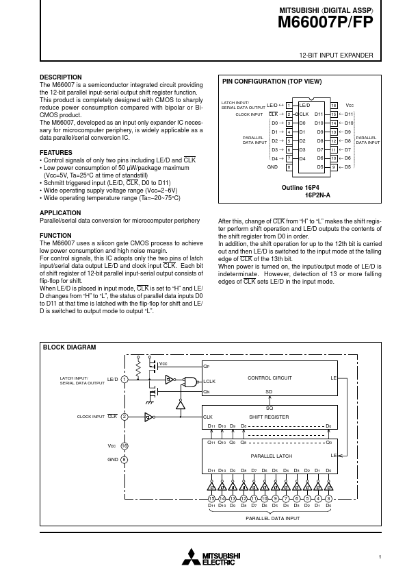
- Wide operating temperature range (Ta=-20~75°C) APPLICATION Parallel/serial data conversion for microcomputer periphery FUNCTION The M66007 uses a silicon gate CMOS process to achieve low power consumption and high noise margin. For control signals, this IC adopts only the two pins of latch input/serial data output LE/D and clock input CLK. Each bit of shift register of 12-bit parallel input-serial output consists of flip-flop for shift. When LE/D is placed in input mode, CLK is set to “H” and LE/ D changes from “H” to “L”, the status of parallel data inputs D0 to D11 at that time is latched with the flip-flop for shift and LE/ D is switched to output mode to output “L”.