M66850FP
M66850FP is SRAM TYPE FIFO MEMORY manufactured by Mitsubishi Electric.
MITSUBISHI <DIGITAL ASSP>
M66850J/FP, M66851J/FP M66852J/FP, M66853J/FP
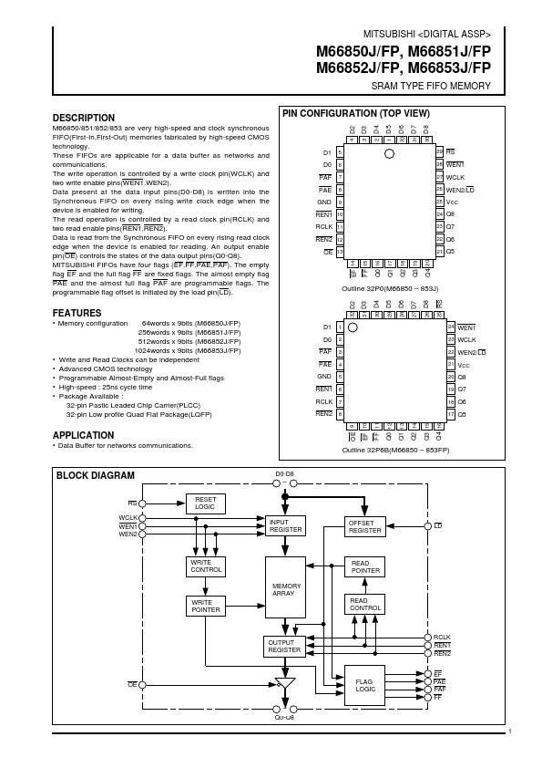
SRAM TYPE FIFO MEMORY PIN CONFIGURATION (TOP VIEW)
2 D4 1 D5 32 D6 31 D7 30 D8 29 RS 28 WEN1 27 WCLK 26 WEN2/LD 25 VCC 24 Q8 23 Q7 22 Q6 21 Q5 4 D2 3 D3
DESCRIPTION
M66850/851/852/853 are very high-speed and clock synchronous FIFO(First-In,First-Out) memories fabricated by high-speed CMOS technology. These FIFOs are applicable for a data buffer as networks and munications. The write operation is controlled by a write clock pin(WCLK) and two write enable pins(WEN1,WEN2). Data present at the data input pins(D0-D8) is written into the Synchronous FIFO on every rising write clock edge when the device is enabled for writing. The read operation is controlled by a read clock pin(RCLK) and two read enable pins(REN1,REN2). Data is read from the Synchronous FIFO on every rising read clock edge when the device is enabled for reading. An output enable pin(OE) controls the states of the data output pins(Q0-Q8). MITSUBISHI FIFOs have four flags (EF,FF,PAE,PAF). The empty flag EF and the full flag FF are fixed flags. The almost empty flag PAE and the almost full flag PAF are programmable flags. The programmable flag offset is initiated by the load pin(LD).
D1 D0 PAF PAE GND
5 6 7 8 9
REN1 10 RCLK 11 REN2 12 OE 13 EF 14 FF 15 Q0 16 Q1 17 Q2 18 Q3 19 Q4 20
Outline 32P0(M66850
- 853J)
25 RS 24 WEN1 23 WCLK 22 WEN2/LD 21 VCC 20 Q8 19 Q7 18 Q6 17 Q5 30 D4 29 D5 28 D6 26 D8 32 D2 31 D3 27 D7
Features
- Memory configuration 64words x 9bits (M66850J/FP) 256words x 9bits (M66851J/FP) 512words x 9bits (M66852J/FP) 1024words x 9bits (M66853J/FP) Write and Read Clocks can be independent Advanced CMOS technology Programmable Almost-Empty and Almost-Full flags High-speed : 25ns cycle time Package Available : 32-pin Pastic Leaded Chip Carrier(PLCC) 32-pin Low profile Quad Flat Package(LQFP)
D1 D0 PAF PAE GND
1 2 3 4 5
- -
- -
- REN1 6 RCLK 7 REN2 8 EF 10 FF 11 Q2 14 Q3 15 Q0 12 OE 9 Q1 13 Q4 16 LD
APPLICATION
-...
Representative M66850FP image (package may vary by manufacturer)