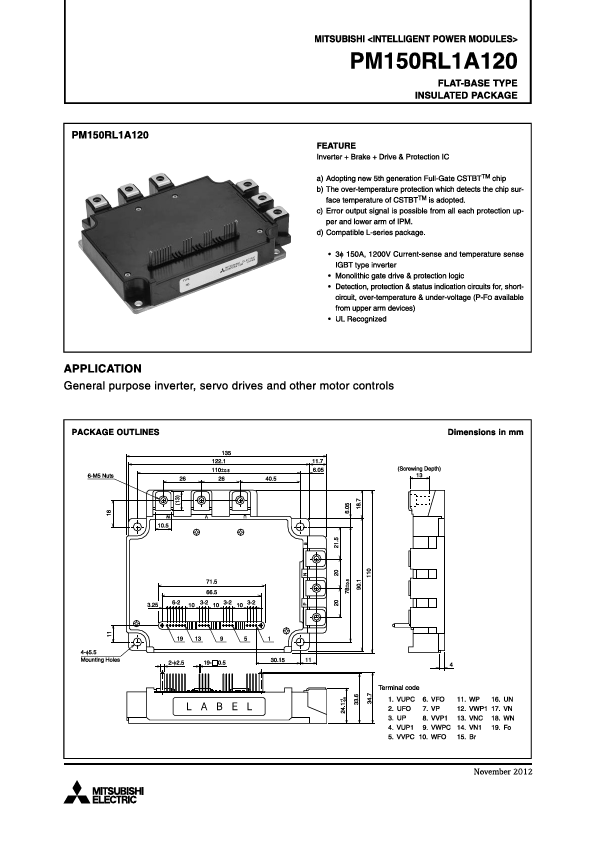
PM150RL1A120 Overview
Key Specifications
Operating Voltage: 15 V
Max Voltage (typical range): 16.5 V
Min Voltage (typical range): 13.5 V
Key Features
- 3φ 150A, 1200V Current-sense and temperature sense IGBT type inverter
- UL Recognized
| Part | PM150RL1A120 |
|---|---|
| Description | INTELLIGENT POWER MODULES |
| Manufacturer | Mitsubishi Electric |
| Size | 3.30 MB |
Operating Voltage: 15 V
Max Voltage (typical range): 16.5 V
Min Voltage (typical range): 13.5 V
| Seller | Inventory | Price Breaks | Buy |
|---|---|---|---|
| Newark | 0 | - | View Offer |
| PLC Direct | 4 | 1+ : 411.91 USD | View Offer |
| Part Number | Manufacturer | Description |
|---|---|---|
| NEO-6M | u-blox | 6 GPS Modules |
| VK2024 | VIKAY | Alphanumeric Dot Matrix Modules |
| ERL35 | FPE | POWER TRANSFORMER MODULES |