FEATURES
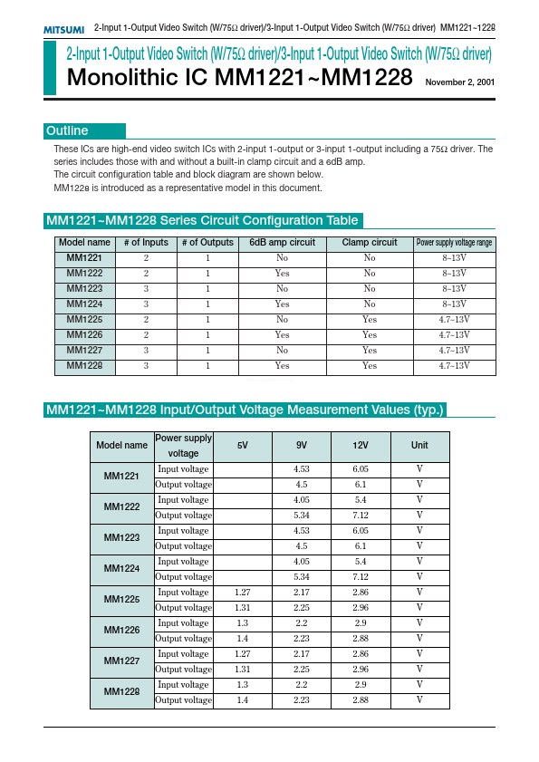
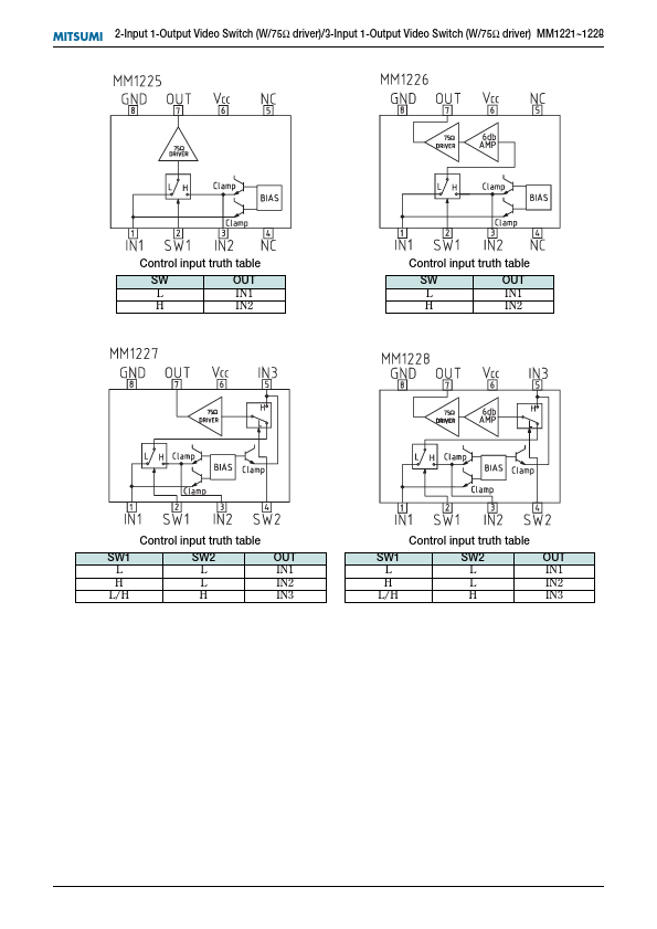
1. 2. 3. 4. 5. 6. 7. 8. 9. Built-in 75Ω driver circuit Built-in 6dB amp Built-in clamp circuit Models in 2. 3. 4. TV VCR Video cameras Other video equipment Block Diagram Control input truth table SW1 L H L/H SW2 L L H OUT IN1 IN2 IN3 MITSUMI 2-Input 1-Output Video Switch (W/75Ω driver)/3-Input 1-Output Video Switch (W/75Ω driver) MM1221~1228 Pin DESCRIPTION
Pin no. 1 3 5 Pin name IN1 IN2 IN3 Function Input Internal equivalent circuit diagram 2 4 SW1 SW2 Switch 7 OUT Output 6 8 VCC GND Power supply Ground MITSUMI 2-Input 1-Output Video Switch (W/75Ω driver)/3-Input 1-Output Video Switch (W/75Ω driver) MM1221~1228 Measuring Circuit ABSOLUTE MAXIMUM RATINGS
Item Storage temperature Operating temperature Power supply voltage Allowable loss (Ta=25°C) Symbol TSTG TOPR VCC Pd Ratings -40~+125 -20~+75 15 300 Units °C °C V mW ELECTRICAL CHARACTERISTICS
Item (Except where noted otherwise, Ta=25°C, VCC=5.0V) Symbol VCC Id GV FC DG DP Voff CT VIH1 VIL1 VIH2 VIL2 Refer to Measuring Circui... Mitsumi Electronics