V55C2128164V
V55C2128164V is 128Mbit LOW-POWER SDRAM manufactured by Mosel Vitelic Corp.
MOSEL VITELIC
V55C2128164V(T/B) 128Mbit LOW-POWER SDRAM 2.5 VOLT, TSOP II / BGA PACKAGE 8M X 16
PRELIMINARY
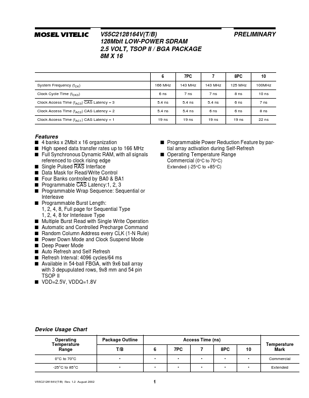
6 System Frequency (fCK) Clock Cycle Time (tCK3) Clock Access Time (tAC3) CAS Latency = 3 Clock Access Time (tAC2) CAS Latency = 2 Clock Access Time (tAC1) CAS Latency = 1 166 MHz 6 ns 5.4 ns 5.4 ns 19 ns
7PC 143 MHz 7 ns 5.4 ns 5.4 ns 19 ns
7 143 MHz 7 ns 5.4 ns 6 ns 19 ns
8PC 125 MHz 8 ns 6 ns 6 ns 19 ns
10 100MHz 10 ns 7 ns 8 ns 22 ns
Features
- 4 banks x 2Mbit x 16 organization
- High speed data transfer rates up to 166 MHz
- Full Synchronous Dynamic RAM, with all signals referenced to clock rising edge
- Single Pulsed RAS Interface
- Data Mask for Read/Write Control
-...