BAV70WT1
Overview
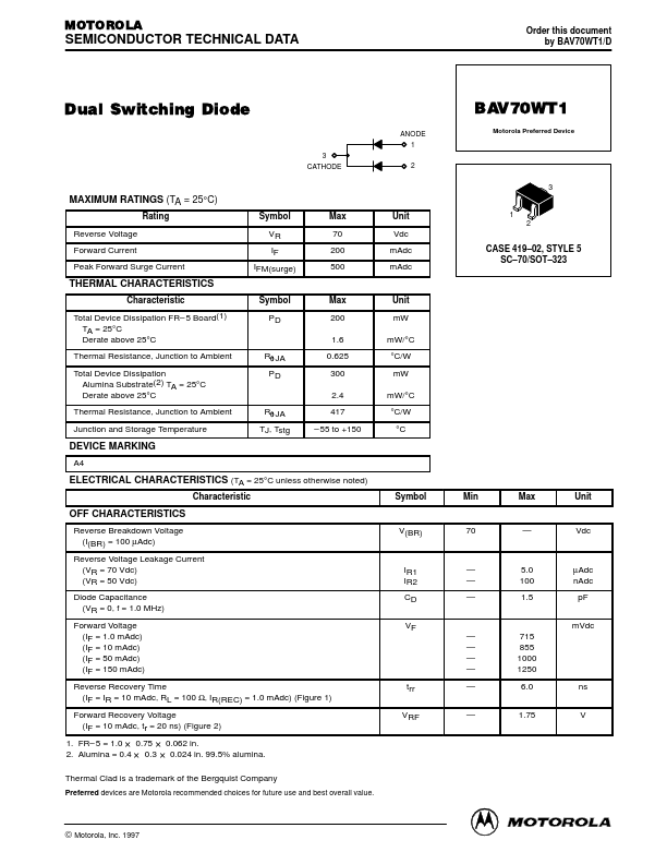
MOTOROLA SEMICONDUCTOR TECHNICAL DATA Order this document by BAV70WT1/D Dual Switching Diode ANODE 1 3 CATHODE 2 BAV70WT1 Motorola Preferred Device 3 MAXIMUM RATINGS (TA = 25°C) Rating Reverse...
| Part | BAV70WT1 |
|---|---|
| Description | Dual Switching Diode |
| Category | Diode |
| Manufacturer | Motorola Semiconductor |
| Size | 107.46 KB |
MOTOROLA SEMICONDUCTOR TECHNICAL DATA Order this document by BAV70WT1/D Dual Switching Diode ANODE 1 3 CATHODE 2 BAV70WT1 Motorola Preferred Device 3 MAXIMUM RATINGS (TA = 25°C) Rating Reverse...
| Part Number | Manufacturer | Description |
|---|---|---|
| BAV70WT1 | onsemi | Dual Switching Diode |
| BAV70WT1 | Leshan Radio Company | Dual Switching Diodes |
| BAV70WT | Micro Commercial Components | Switching Diode |
| BAV70W | onsemi | Dual Switching Diode Common Cathode |
| BAV70W | Nexperia | High-speed switching double diode |