BC559C
MOTOROLA
SEMICONDUCTOR TECHNICAL DATA
Low Noise Transistors
Order this document by BC559/D
PNP Silicon
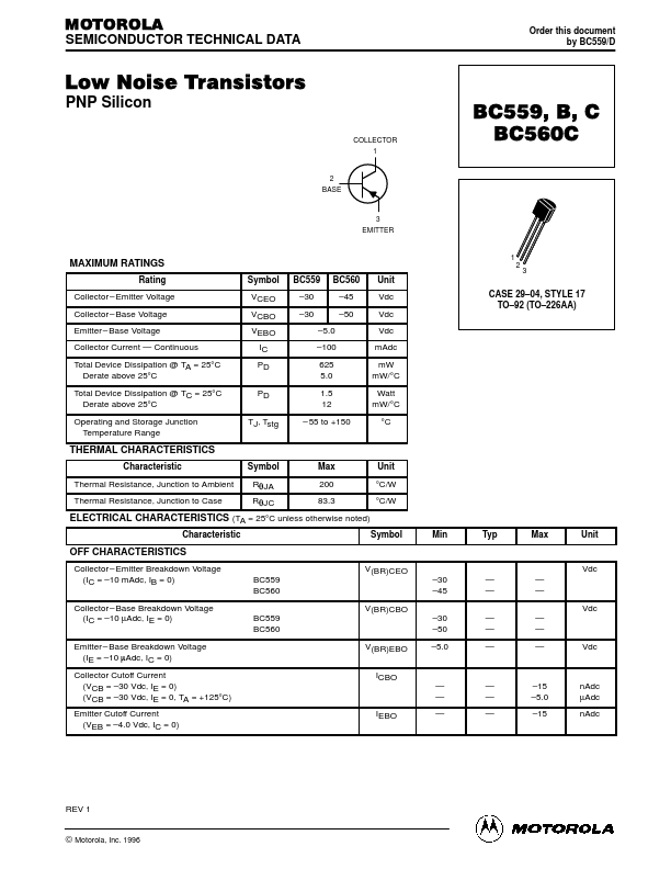
COLLECTOR 1 2 BASE 3 EMITTER
BC559, B, C BC560C
MAXIMUM RATINGS
Rating Collector
- Emitter Voltage Collector
- Base Voltage Emitter
- Base Voltage Collector Current
- Continuous Total Device Dissipation @ TA = 25°C Derate above 25°C Total Device Dissipation @ TC = 25°C Derate above 25°C Operating and Storage Junction Temperature Range Symbol VCEO VCBO VEBO IC PD PD TJ, Tstg BC559
- 30
- 30
- 5.0
- 100 625 5.0 1.5 12
- 55 to +150 BC560
- 45
- 50 Unit Vdc Vdc Vdc m Adc m W m W/°C Watt m W/°C °C
1 2 3
CASE 29- 04, STYLE 17 TO- 92 (TO- 226AA)
THERMAL CHARACTERISTICS
Characteristic Thermal Resistance, Junction to Ambient Thermal Resistance, Junction to Case Symbol Rq JA Rq JC Max 200 83.3 Unit °C/W °C/W
ELECTRICAL CHARACTERISTICS (TA = 25°C unless otherwise noted)
Characteristic Symbol Min Typ Max Unit
OFF CHARACTERISTICS
Collector
- Emitter Breakdown Voltage (IC =
- 10 m Adc, IB = 0) Collector
-...