PC33253DW
PC33253DW is Full Bridge Pre-Driver manufactured by Motorola Semiconductor.
feature
, associated to external capacitor provides a full floating high side drive. An under- and over-voltage protection prevents erratic system operation at abnormal supply voltages. Under fault, these functions force the driver stages into off state. The logic inputs are patible with standard CMOS or LSTTL outputs. The input hysteresis makes the output switching time independent of the input transition time. The global enable logic signal can be used to disable the charge pump and all the bias circuit. The net advantage is the reduction of the quiescent supply current to under 10µA. To wake up the circuit, 5 V has to be provided at G_EN. A built-in single supply operational amplifier could be used to feedback information from the output load to the external MCU.
- VCC Operating Voltage Range from 5.5 V up to 55 V
- VCC2 Operating Voltage Range from 5.5 V up to 28 V
- Automotive Temperature Range -40°C to 125°C
- 1A Pulse Current Output Driver
- Fast PWM Capability
- Built-In Charge Pump
- Cross Conduction Suppression Circuit
Freescale Semiconductor, Inc...
DW SUFFIX
PLASTIC PACKAGE CASE 751F-05
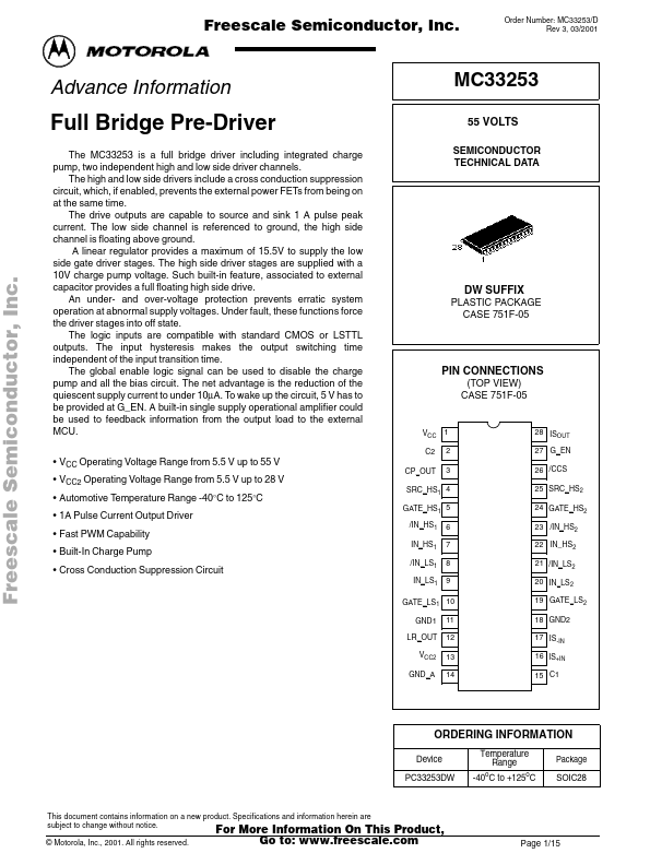
PIN CONNECTIONS
(TOP VIEW) CASE 751F-05
VCC C2 CP_OUT
1 2 3
28 ISOUT 27 G_EN 26 /CCS 25 SRC_HS2 24 GATE_HS2 23 /IN_HS2 22 IN_HS2 21 /IN_LS2 20 IN_LS2 19 GATE_LS2 18 GND2 17 IS-IN 16 IS+IN 15 C1
SRC_HS1 4 GATE_HS1 5 /IN_HS1 IN_HS1 /IN_LS1 IN_LS1 6 7 8 9
GATE_LS1 10 GND1 LR_OUT VCC2 GND_A 11 12 13 14
ORDERING INFORMATION
Device PC33253DW Temperature Range -40o C to +125o C
Package
SOIC28
This document contains information on a new product. Specifications and information herein are subject to change without notice. © Motorola, Inc., 2001. All rights reserved.
For More Information On This Product, Go to: .freescale.
Page 1/15
MC33253 Freescale Semiconductor, Inc. Figure 1. Principal Building Blocks
Ccp C1 VCC UV/OV Detect VDD VCC VCC RDY EN GND G_EN VCC2 VCC2 +13.5 V VDD CP_OUT CLR_OUT LR_OUT Vgs_hs Charge Pump C1 C2 Vpos +13.5 V CCP_OUT 5.5 V... 55 V Linear +5.0...