Datasheet4U Logo Datasheet4U.com

SN54LS174 Datasheet Hex D Flip-flop

Manufacturer: Motorola Semiconductor (now NXP Semiconductors)

Overview: 
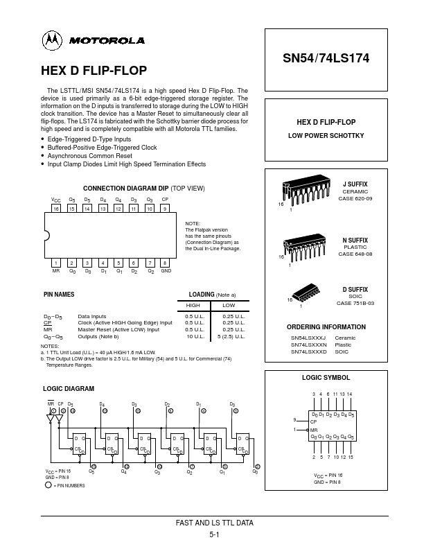
SN54/74LS174 HEX D FLIP-FLOP The LSTTL / MSI SN54 / 74LS174 is a high speed Hex D Flip-Flop. The device is used primarily as a 6-bit edge-triggered storage register. The information on the D inputs is transferred to storage during the LOW to HIGH clock transition. The device has a Master Reset to simultaneously clear all flip-flops. The LS174 is fabricated with the Schottky barrier diode process for high speed and is completely compatible with all Motorola TTL families. HEX D FLIP-FLOP LOW POWER SCHOTTKY • • • • Edge-Triggered D-Type Inputs Buffered-Positive Edge-Triggered Clock Asynchronous Common Reset Input Clamp Diodes Limit High Speed Termination Effects CONNECTION DIAGRAM DIP (TOP VIEW) VCC 16 Q5 15 D5 14 D4 13 Q4 12 D3 11 Q3 10 CP 9 NOTE: The Flatpak version has the same pinouts (Connection Diagram) as the Dual In-Line Package. 16 16 1 J SUFFIX CERAMIC CASE 620-09 N SUFFIX PLASTIC CASE 648-08 1 1 MR 2 Q0 3 D0 4 D1 5 Q1 6 D2 7 Q2 8 GND PIN NAMES LOADING (Note a) 16 HIGH D0 – D5 CP MR Q0 – Q5 Data Inputs Clock (Active HIGH Going Edge) Input Master Reset (Active LOW) Input Outputs (Note b) 0.5 U.L. 0.5 U.L. 0.5 U.L. 10 U.L. LOW 0.25 U.L. 0.25 U.L. 0.25 U.L. 5 (2.5) U.L. 1 D SUFFIX SOIC CASE 751B-03 ORDERING INFORMATION SN54LSXXXJ SN74LSXXXN SN74LSXXXD Ceramic Plastic SOIC NOTES: a. 1 TTL Unit Load (U.L.) = 40 µA HIGH/1.6 mA LOW. b. The Output LOW drive factor is 2.5 U.L. for Military (54) and 5 U.L. for Commercial (74) b. Temperature Ranges.

General Description

The LS174 consists of six edge-triggered D flip-flops with individual D inputs and Q outputs.

The Clock (CP) and Master

SN54LS174 Distributor & Price

Compare SN54LS174 distributor prices and check real-time stock availability from major suppliers. Prices and inventory may vary by region and order quantity.