2N4093
Overview
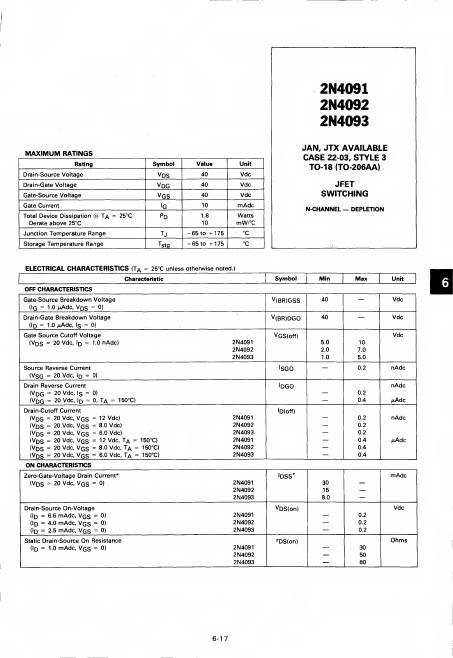
2N4091 2N4092 2N4093 MAXIMUM RATINGS Rating Drain-Source Voltage Drain-Gate Voltage Gate-Source Voltage Gate Current @Total Device Dissipation Ta = 25°C Derate above 25°C Junction Temperature Range S...
| Part | 2N4093 |
|---|---|
| Description | JFET |
| Manufacturer | Motorola Semiconductor |
| Size | 54.33 KB |
2N4091 2N4092 2N4093 MAXIMUM RATINGS Rating Drain-Source Voltage Drain-Gate Voltage Gate-Source Voltage Gate Current @Total Device Dissipation Ta = 25°C Derate above 25°C Junction Temperature Range S...
| Part Number | Manufacturer | Description |
|---|---|---|
| 2N4093 | Microsemi | N-CHANNEL J-FET |
| 2N4093 | Taitron Components | N-Channel Metal Can JFET |
| 2N4093 | InterFET | N-Channel JFET |
| 2N4092 | Microsemi | N-CHANNEL J-FET |
| 2N4091 | Microsemi | N-CHANNEL J-FET |