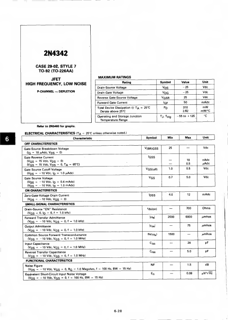
2N4342 Overview
Key Specifications
Max Operating Temp: 125 °C
Key Features
- 10 Vdc, lp = 1.0 fiAdc)
| Part | 2N4342 |
|---|---|
| Description | P-CHANNEL JFET |
| Manufacturer | Motorola Semiconductor |
| Size | 32.39 KB |
Max Operating Temp: 125 °C
| Seller | Inventory | Price Breaks | Buy |
|---|---|---|---|
| Classic Components | 3 | - | View Offer |
| Part Number | Manufacturer | Description |
|---|---|---|
| 2N4347 | Inchange Semiconductor | NPN Transistor |
| 2N4341 | Calogic LLC | N-Channel JFET |
| 2N4340 | InterFET | N-Channel JFET |
| 2N4340 | Calogic LLC | N-Channel JFET |
| 2N4340 | Vishay | N-Channel JFETs |