Motorola 2N4921
MEDIUM-POWER PLASTIC NPN SILICON TRANSISTORS
| Part No. | 2N4921 |
|---|---|
| Datasheet | 2N4921 Download |
| Manufacturer |  Motorola |
| Description | MEDIUM-POWER PLASTIC NPN SILICON TRANSISTORS |
| Buy | Stock & Price |
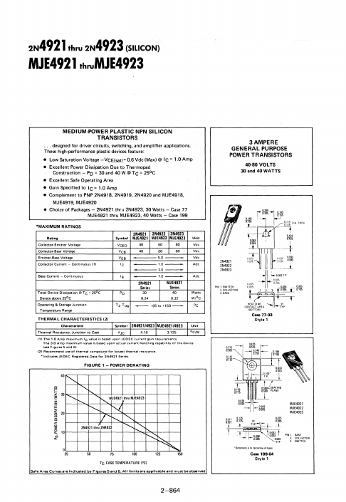
MAXIMUM RATINGS
Rating Collector-Emitter Voltage Collector-Base Voltage Emitter-Base Voltage Collector Current Continuous (11 Base Current Continuous Total Device Dissipation @TC '" 25D C Derate above 2SoC Operating & Storage Junction Temperature Range 2N4921 2N4922 2N4923 Symbol MJE4921 MJE4922 MJE4923 VeEO VeB VEe Ie Ie Po 40 40 2N4921 Series 30 0.24 60 80 60 80 5.0 1.0 3.0 1.0_ MJE4921 Series 40 0.32 TJ, Tstg - - -65 to +150-- Unit Vdc Vdc Vdc Adc Adc Watts WIDe °e THERMAL CHARACTERISTICS (2) Characteristic Thermal Resistance, Junction to Case (1) The 1.0 Amp maximum Ie value is based upon JEDEC current gain requirements. The 3.0 Amp maximum value is based upon actual current-handling capability of the device (see Figure. 5 and 6). (2) Recommend use of thermal compou~d for lowest thermal resistance.●'ndicates JEDEC Registered Data for 2N4921 Series. FIGURE 1 - POWER DERATING 40 '"""" '"""'~ ........... ...... ' " MJE4921thru MJE4923 .......... I'---- ~ r ""- '"'" 2N4921thru 2N4923 ............