Motorola 4N30
4N33 is JEDEC Registration for VISO only. The same applies for 4N29 and 4N30. For this test, Pins 1 and 2 are common, and Pins 4, 5 and 6 are common.| Part No. | 4N30 |
|---|---|
| Datasheet | 4N30 Download |
| Manufacturer |  Motorola |
| Description | 6-Pin DIP Optoisolators |
| Buy | Stock & Price |
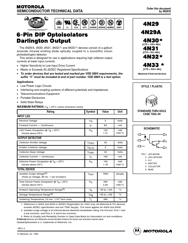
APPLICATIONS
● Low Power Logic Circuits● Interfacing and coupling systems of different potentials and impedances
● Telecommunications Equipment
● Portable Electronics
● Solid State Relays
MAXIMUM RATINGS
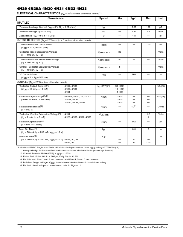
(TA = 25°C unless otherwise noted) Rating INPUT LED Reverse Voltage Forward Current — Continuous LED Power Dissipation @ TA = 25°C Derate above 25°C OUTPUT DETECTOR Collector–Emitter Voltage Emitter–Collector Voltage Collector–Base Voltage Collector Current — Continuous Detector Power Dissipation @ TA = 25°C Derate above 25°C TOTAL DEVICE Isolation Surge Voltage(2) (Peak ac Voltage, 60 Hz, 1 sec Duration) Total Device Power Dissipation @ TA = 25°C Derate above 25°C Ambient Operating Temperature Range(3) Storage Temperature Range(3) Soldering Temperature (10 sec, 1/16″ from case) VISO PD TA Tstg TL 7500 250 2.94 – 55 to +100 – 55 to +150 260 Vac(pk) mW mW/°C °C °C °C VCEO VECO VCBO IC PD 30 5 30 150 150 1.76 Volts Volts Volts mA mW mW/°C VR IF PD 3 60 120 1.41 Volts mA mW mW/°C Symbol...