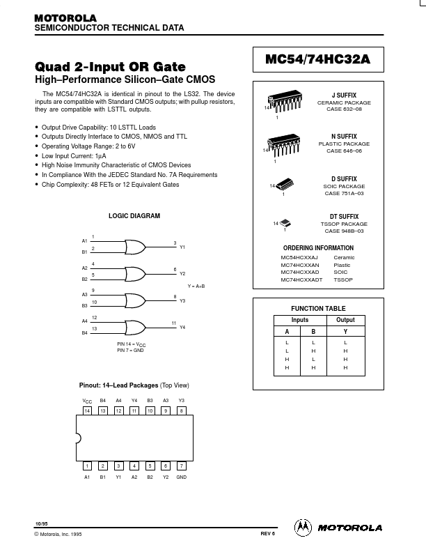
Motorola 54HC32
Quad 2-Input OR Gate
| Part No. | 54HC32 |
|---|---|
| Datasheet | 54HC32 Download |
| Manufacturer |  Motorola |
| Description | Quad 2-Input OR Gate |
| Buy | Stock & Price |
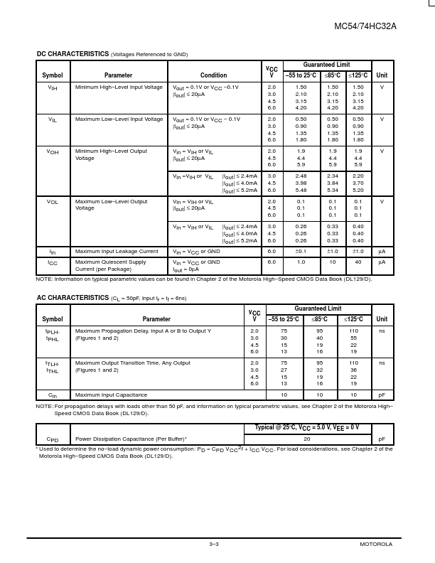
MAXIMUM RATINGS
are those values beyond which damage to the device may occur. This device contains protection circuitry to guard against damage due to high static voltages or electric fields. However, precautions must be taken to avoid applications of any voltage higher than maximum rated voltages to this high–impedance cir- cuit. For proper operation, Vin and v vVout should be constrained to the range GND (Vin or Vout) VCC. Unused inputs must always be tied to an appropriate logic voltage level (e.g., either GND or VCC). Unused outputs must be left open. Functional operation should be restricted to the Recommended Operating Conditions. †Derating — Plastic DIP: – 10 mW/_C from 65_ to 125_C Ceramic DIP: – 10 mW/_C from 100_ to 125_C SOIC Package: – 7 mW/_C from 65_ to 125_C TSSOP Package: – 6.1 mW/_C from 65_ to 125_C ÎÎÎÎÎÎÎÎÎÎÎÎÎÎÎÎÎÎÎÎÎÎÎFor high frequency or heavy load considerations, see Chapter 2 of the Motorola High–Speed CMOS Data Book (DL129/D). ÎÎÎÎÎÎÎÎÎÎÎÎÎÎÎÎÎÎÎÎÎÎÎRECOMMEND...