ELECTRICAL CHARACTERISTICS
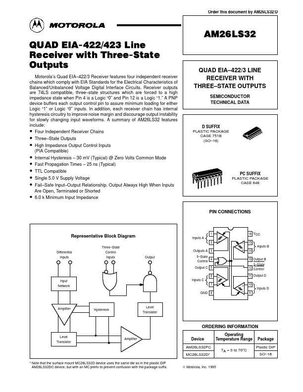
of Balanced/Unbalanced Voltage Digital Interface Circuits. Receiver outputs are 74LS compatible, three–state structures which are forced to a high impedance state when Pin 4 is a Logic “0” and Pin 12 is a Logic “1.” A PNP device buffers each output control pin to assure minimum loading for either Logic “1” or Logic “0” inputs. In addition, each receiver chain has internal hysteresis circuitry to improve noise margin and discourage output instability for slowly changing input waveforms. A summary of Output Always High When Inputs Are Open, Terminated or Shorted 6.0 k Minimum Input Impedance D SUFFIX PLASTIC PACKAGE CASE 751B (SO–16) PC SUFFIX PLASTIC PACKAGE CASE 648 PIN CONNECTIONS Representative Block Diagram Three–State Control Inputs 1 – + – + 16 VCC 15 Inputs A 2 Inputs B 14 13 Output B 12 Differential Inputs Output Outputs A 3 3–State Control 4 Output C 5 6 3–State Control Input Network Inputs C 7 + – + – 11 Output D 10 Inputs D 9 GND 8 Amplifier Hystere... Motorola