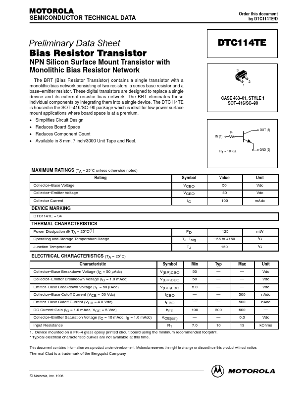
MAXIMUM RATINGS
(TA = 25°C unless otherwise noted) Rating Collector–Base Voltage Collector–Emitter Voltage Collector Current Symbol VCBO VCEO IC Value 50 50 100 Unit Vdc Vdc mAdc DEVICE MARKING DTC114TE = 94 THERMAL CHARACTERISTICS Power Dissipation @ TA = 25°C(1) Operating and Storage Temperature Range Junction Temperature PD TJ, Tstg TJ *125 – 55 to +150 150 mW °C °C ELECTRICAL CHARACTERISTICS
(TA = 25°C) Characteristic Collector–Base Breakdown Voltage (IC = 50 µAdc) Collector–Emitter Breakdown Voltage (IC = 1.0 mAdc) Emitter–Base Breakdown Voltage (IE = 50 µAdc) Collector–Base Cutoff Current (VCB = 50 Vdc) Emitter–Base Cutoff Current (VEB = 4.0 Vdc) DC Current Gain (IC = 1.0 mAdc, VCE = 5 Vdc) Collector–Emitter Saturation Voltage (IC = 10 mAdc, IB = 1.0 mAdc) Input Resistance Symbol V(BR)CBO V(BR)CEO V(BR)EBO ICBO IEBO hFE VCE(sat) R1 Min 50 50 5.0 — — 100 — 7.0 Typ — — — — — 300 — 10 Max — — — 500 500 600 0.3 13 Unit Vdc Vdc Vdc nAdc nAdc — Vdc kOhms 1. Device mounted on a FR–4 glass epoxy printed circuit board using the minimum recommended footprint. * Typical electrical characteristic curves are not available at this time. Motorola