J201
Overview
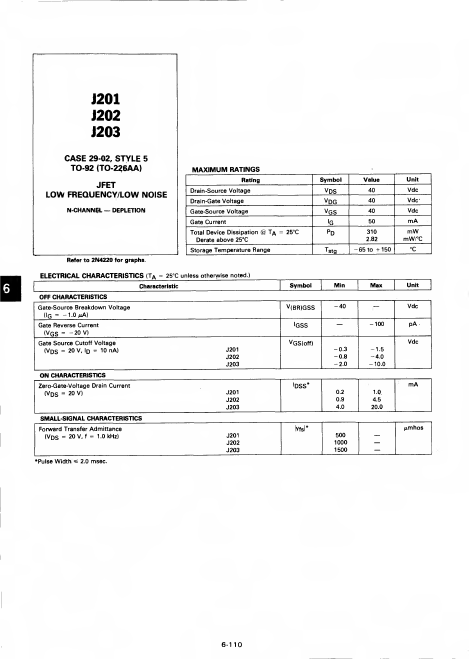
J201 J202 J203 CASE 29-02, STYLE 5 TO-92 (TO-226AA) JFET LOW FREQUENCY/LOW NOISE —N-CHANNEL DEPLETION Refer to 2N4220 for graphs. MAXIMUM RATINGS Rating Drain-Source Voltage Drain-Gate Voltage Gate-...
| Part | J201 |
|---|---|
| Description | LOW FREQUENCY/LOW NOISE JFET |
| Manufacturer | Motorola Semiconductor |
| Size | 25.18 KB |
J201 J202 J203 CASE 29-02, STYLE 5 TO-92 (TO-226AA) JFET LOW FREQUENCY/LOW NOISE —N-CHANNEL DEPLETION Refer to 2N4220 for graphs. MAXIMUM RATINGS Rating Drain-Source Voltage Drain-Gate Voltage Gate-...