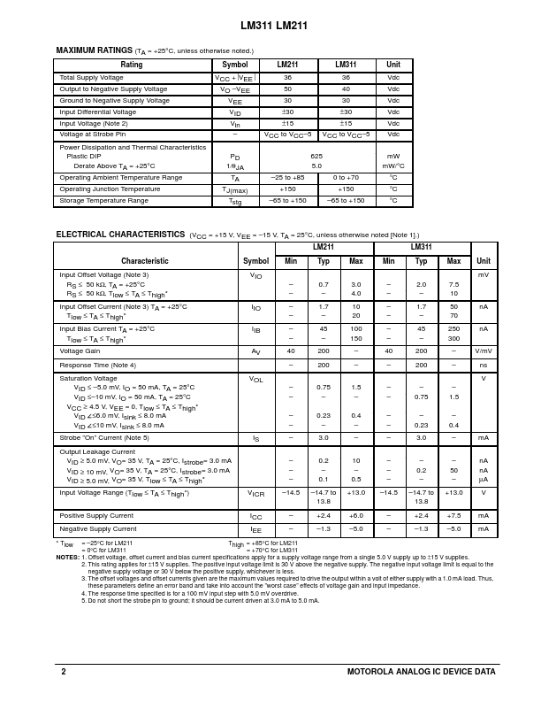
MAXIMUM RATINGS
(TA = +25°C, unless otherwise noted.) Rating Total Supply Voltage Output to Negative Supply Voltage Ground to Negative Supply Voltage Input Differential Voltage Input Voltage (Note 2) Voltage at Strobe Pin Power Dissipation and Thermal Characteristics Plastic DIP Derate Above TA = +25°C Operating Ambient Temperature Range Operating Junction Temperature Storage Temperature Range Symbol VCC +VEE VO –VEE VEE VID Vin – PD 1/θJA TA TJ(max) Tstg –25 to +85 +150 –65 to +150 LM211 36 50 30 ±30 ±15 VCC to VCC–5 LM311 36 40 30 ±30 ±15 VCC to VCC–5 Unit Vdc Vdc Vdc Vdc Vdc Vdc mW mW/°C 0 to +70 +150 –65 to +150 °C °C °C 625 5.0 ELECTRICAL CHARACTERISTICS
(VCC = +15 V, VEE = –15 V, TA = 25°C, unless otherwise noted [Note 1].) LM211 Ch Characteristic i i Input Offset Voltage (Note 3) RS ≤ 50 kΩ, TA = +25°C RS ≤ 50 kΩ, Tlow ≤ TA ≤ Thigh* Input Offset Current (Note 3) TA = +25°C Tlow ≤ TA ≤ Thigh* Input Bias Current TA = +25°C Tlow ≤ TA ≤ Thigh* Voltage Gain Response Time (Note 4) S... Motorola