Datasheet Details
| Part number | MC100LVEL14 |
|---|---|
| Manufacturer | Motorola Semiconductor (now NXP Semiconductors) |
| File Size | 83.17 KB |
| Description | 1:5 Clock Distribution Chip |
| Datasheet | MC100LVEL14-Motorola.pdf |
|
|
|
Overview: MOTOROLA SEMICONDUCTOR TECHNICAL DATA 1:5 Clock Distribution Chip 
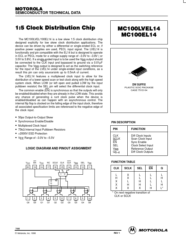
The MC100LVEL/100EL14 is a low skew 1:5 clock distribution chip designed explicitly for low skew clock distribution applications. The device can be driven by either a differential or single-ended ECL or, if positive power supplies are used, PECL input signal. The LVEL14 is functionally and pin patible with the EL14 but is designed to operate in ECL or PECL mode for a voltage supply range of –3.0V to –3.8V ( or 3.0V to 3.8V). If a single-ended input is to be used the VBB output should be connected to the CLK input and bypassed to ground via a 0.01µF capacitor. The VBB output is designed to act as the switching reference for the input of the LVEL14 under single-ended input conditions, as a result this pin can only source/sink up to 0.5mA of current.
| Part number | MC100LVEL14 |
|---|---|
| Manufacturer | Motorola Semiconductor (now NXP Semiconductors) |
| File Size | 83.17 KB |
| Description | 1:5 Clock Distribution Chip |
| Datasheet | MC100LVEL14-Motorola.pdf |
|
|
|
| Brand Logo | Part Number | Description | Manufacturer |
|---|---|---|---|
| MC100LVEL14 | 1:5 Clock Distribution Chip | ON Semiconductor |
| Part Number | Description |
|---|---|
| MC100LVEL11 | Low Voltage 1:2 Differential Fanout Buffer |
| MC100LVEL12 | Low Impedance Driver |
| MC100LVEL13 | Dual 1:3 Fanout Buffer |
| MC100LVEL16 | Differential Receiver |
| MC100LVEL17 | Low-Voltage Quad Differential Receiver |
| MC100LVEL01 | 4-Input OR/NOR |
| MC100LVEL05 | 2-Input Differential AND/NAND |
| MC100LVEL29 | Dual Differential Data and Clock D Flip-Flop |
| MC100LVEL30 | Triple D Flip-Flop |
| MC100LVEL31 | D Flip-Flop |