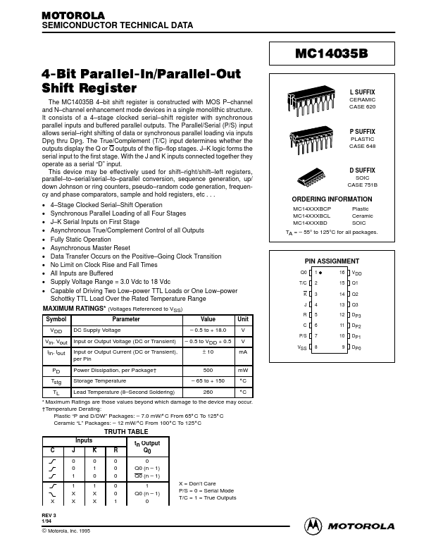
MAXIMUM RATINGS
* (Voltages Referenced to VSS) Symbol VDD DC Supply Voltage Unit V V – 0.5 to + 18.0 Vin, Vout lin, lout PD Input or Output Voltage (DC or Transient) – 0.5 to VDD + 0.5 ± 10 500 Input or Output Current (DC or Transient), per Pin Power Dissipation, per Package† Storage Temperature mA mW Tstg TL – 65 to + 150 260 _C _C Lead Temperature (8–Second Soldering) * MAXIMUM RATINGS
are those values beyond which damage to the device may occur. †Temperature Derating: Plastic “P and D/DW” Packages: – 7.0 mW/_C From 65_C To 125_C Ceramic “L” Packages: – 12 mW/_C From 100_C To 125_C TRUTH TABLE Inputs C J 0 0 1 1 X X K 0 1 0 1 X X R 0 0 0 0 0 1 tn Output Q0 0 Q0 (n – 1) Q0 (n – 1) 1 Q0 (n – 1) 0 X = Don’t Care P/S = 0 = Serial Mode T/C = 1 = True Outputs X REV 3 1/94 ©MC14035B Motorola, Inc. 1995 144 MOTOROLA CMOS LOGIC DATA ÎÎÎÎÎÎÎÎÎÎÎÎÎÎÎÎÎÎÎÎÎÎÎÎÎÎÎÎÎÎÎÎÎÎ ÎÎÎÎÎÎÎÎÎÎÎÎÎÎÎÎÎÎÎÎÎÎÎÎÎÎÎÎÎÎÎÎÎÎ ÎÎÎÎÎÎÎÎÎÎ ÎÎÎÎ ÎÎÎ ÎÎÎÎÎÎ ÎÎÎÎÎÎÎÎ ÎÎÎÎÎÎ ÎÎÎ ÎÎÎÎÎÎÎÎÎÎÎÎÎÎÎÎÎÎÎÎÎÎÎÎÎÎÎÎÎÎÎÎÎÎ ÎÎÎÎÎÎ ÎÎÎÎ... Motorola