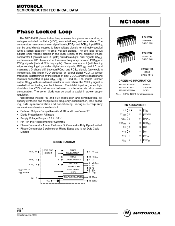
MC14046B
Key Features
- controlled oscillator (VCO), source follower, and zener diode. The parators have two mon signal inputs, PCAin and PCBin. Input PCAin can be used directly coupled to large voltage signals, or indirectly coupled (with a series capacitor) to small voltage signals. The self
- bias circuit adjusts small voltage signals in the linear region of the amplifier. Phase parator 1 (an exclusive OR gate) provides a digital error signal PC1out, and maintains 90° phase shift at the center frequency between PCAin and PCBin signals (both at 50% duty cycle). Phase parator 2 (with leading edge sensing logic) provides digital error signals, PC2 out and LD, and maintains a 0° phase shift between PCA in and PCB in signals (duty cycle is immaterial). The linear VCO produces an output signal VCO out whose frequency is determined by the voltage of input VCO in and the capacitor and resistors connected to pins C1A, C1B, R1, and R2. The source