Datasheet4U Logo Datasheet4U.com

MC145151 - Parallel-Input PLL Frequency Synthesizer

General Description

INPUT PINS fin Frequency Input (Pin 1) Input to the ÷ N portion of the synthesizer.

fin is typically derived from loop VCO and is ac coupled into the device.

For larger amplitude signals (standard CMOS logic levels) dc coupling may be used.

RA2 Reference Address Inputs (Pins 5, 6, 7)

Key Features

  • consist of a reference oscillator, selectable.
  • reference divider, digital.
  • phase detector, and 14.
  • bit programmable divide.
  • by.
  • N counter. The MC145151.
  • 2 is an improved.
  • performance drop.
  • in replacement for the MC145151.
  • 1. The power consumption has decreased and ESD and latch.
  • up performance have improved.

📥 Download Datasheet

Full PDF Text Transcription (Reference)

The following content is an automatically extracted verbatim text from the original manufacturer datasheet and is provided for reference purposes only.

View original datasheet text
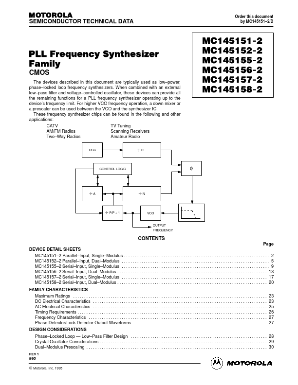
MOTOROLA SEMICONDUCTOR TECHNICAL DATA Order this document by MC145151–2/D PLL Frequency Synthesizer Family CMOS The devices described in this document are typically used as low–power, phase–locked loop frequency synthesizers. When combined with an external low–pass filter and voltage–controlled oscillator, these devices can provide all the remaining functions for a PLL frequency synthesizer operating up to the device’s frequency limit. For higher VCO frequency operation, a down mixer or a prescaler can be used between the VCO and the synthesizer IC.