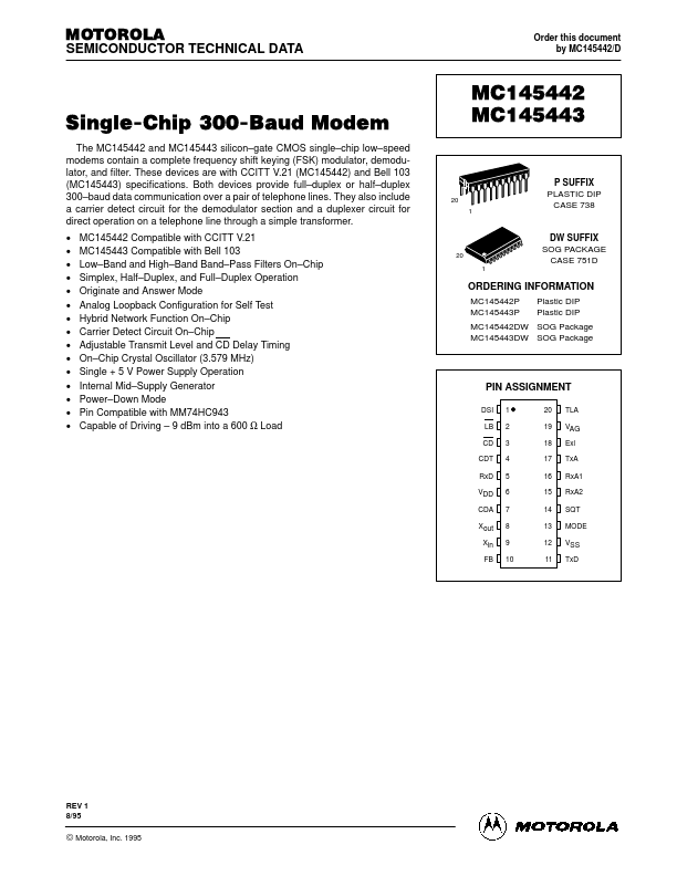
MC145443
description
.
ABSOLUTE MAXIMUM RATINGS (Voltages Referenced to VSS)
Rating Supply Voltage DC Input Voltage DC Output Voltage Clamp Diode Current, per Pin DC Output Current, per Pin Power Dissipation Operating Temperature Range Storage Temperature Range Symbol VDD Vin Vout IIK, IOK Iout PD TA Tstg Value
- 0.5 to + 7.0
- 0.5 to VDD + 0.5
- 0.5 to VDD + 0.5 ± 20 ± 28 500
- 40 to + 85
- 65 to + 150 Unit V V V m A m A m W °C °C This device contains circuitry to protect the inputs against damage due to high static voltages or electric fields; however, it is advised that normal precautions be taken to avoid application of any voltage higher than maximum rated voltages to this high impedance circuit. For proper operation it is remended that Vin and Vout be constrained to the range VSS ≤ (Vin or Vout) ≤ VDD). Unused inputs must always be tied to an appropriate logic voltage level (e.g., either VSS or VDD).
REMENDED OPERATING CONDITIONS
Parameter Supply Voltage DC Input or Output Voltage Input...