MC145583
MOTOROLA
SEMICONDUCTOR TECHNICAL DATA
Order this document by MC145583/D
Product Preview
3.3 Volt Only Driver/Receiver with an Integrated Standby Mode
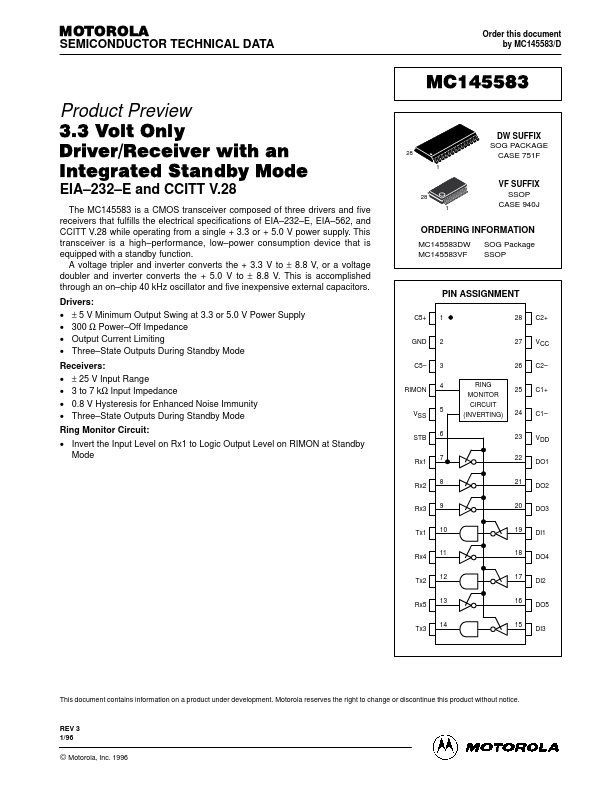
28 1
DW SUFFIX SOG PACKAGE CASE 751F
EIA- 232- E and CCITT V.28
The MC145583 is a CMOS transceiver posed of three drivers and five receivers that fulfills the electrical specifications of EIA- 232- E, EIA- 562, and CCITT V.28 while operating from a single + 3.3 or + 5.0 V power supply. This transceiver is a high- performance, low- power consumption device that is equipped with a standby function. A voltage tripler and inverter converts the + 3.3 V to ± 8.8 V, or a voltage doubler and inverter converts the + 5.0 V to ± 8.8 V. This is acplished through an on- chip 40 k Hz oscillator and five inexpensive external capacitors. Drivers:
- ± 5 V Minimum Output Swing at 3.3 or 5.0 V Power Supply
- 300 Ω Power- Off Impedance
- Output Current Limiting
- Three- State Outputs During Standby Mode Receivers:
- ± 25 V Input Range
- 3 to 7 kΩ Input...