MC74AC299
DESCRIPTION
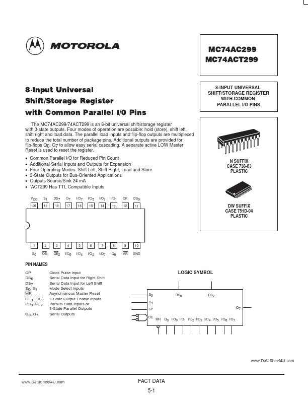
The MC74AC299/74ACT299 contains eight edge-triggered D-type flip-flops and the interstage logic necessary to perform synchronous shift left, shift right, parallel load and hold operations. The type of operation is determined by S0 and S1, as shown in the Truth Table. All flip-flop outputs are brought out through 3-state buffers to separate I/O pins that also serve as data inputs in the parallel load mode. Q0 and Q7 are also brought out on other pins for expansion in serial shifting of longer words. A LOW signal on MR overrides the Select and CP inputs and resets the flip-flops. All other state changes are initiated by the rising edge of the clock. Inputs can change when the clock is in either state provided only that the remended setup and hold times, relative to the rising edge of CP, are observed. A HIGH signal on either OE1 or OE2 disables the 3-state buffers and puts the I/O pins in the high impedance state. In this condition the shift, hold, load and reset operations...