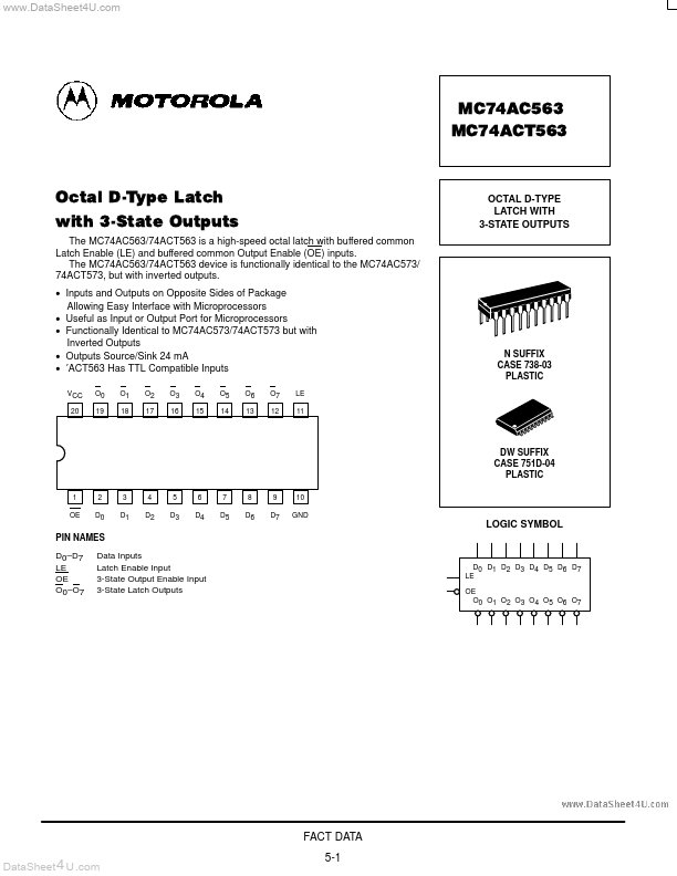
MC74AC563
MC74AC563 is OCTAL D-TYPE LATCH manufactured by Motorola Semiconductor.
DESCRIPTION
The MC74AC563/74ACT563 contains eight D-type latches with 3-state plementary outputs. When the Latch Enable (LE) input is HIGH, data on the D n inputs enters the latches. In this condition the latches are transparent, i.e., a latch output will change state each time its D input changes. When LE is LOW the latches store the information that was present on the D inputs a setup time preceding the HIGH-to-LOW transition of LE. The 3-state buffers are controlled by the Output Enable (OE) input. When OE is LOW, the buffers are in the bi-state mode. When OE is HIGH the buffers are in the high impedance mode but that does not interfere with entering new data into the latches. FUNCTION TABLE
Inputs OE H H H H L L L LE X H H L H H L D X L H X L H X Internal Q X H L NC H L NC Outputs Function O Z Z Z Z H L NC High Z High Z High Z Latched Transparent Transparent Latched
H = HIGH Voltage Level L = LOW Voltage Level X = Immaterial Z = High Impedance NC = No Change
LOGIC DIAGRAM
D0 D1 D2 D3 D4 D5 D6 D7
C LE
OE O1 O2 O3 O4 O5 O6 O7 O8
Please note that this diagram is provided only for the understanding of logic operations and should not be used to estimate propagation delays.
FACT DATA
Data Sheet 4 U .
5-2
..
MC74AC563 MC74ACT563
MAXIMUM RATINGS-
Symbol VCC Vin Vout Iin Iout ICC Tstg Parameter DC Supply Voltage (Referenced to GND) DC Input Voltage (Referenced to GND) DC Output Voltage (Referenced to GND) DC Input Current, per Pin DC Output Sink/Source Current, per Pin DC VCC or GND Current per Output Pin Storage Temperature Value
- 0.5 to +7.0
- 0.5 to VCC +0.5
- 0.5 to VCC +0.5 ±20 ±50 ±50
- 65 to +150 Unit V V V m A m A m A °C
- Maximum Ratings are those values beyond which damage to the device may occur. Functional operation should be restricted to the Remended Operating...