• Part: MC74AC646
  • Description: OCTAL TRANSCEIVER/REGISTER
  • Manufacturer: Motorola Semiconductor
  • Size: 253.67 KB
Download MC74AC646 Datasheet PDF
Motorola Semiconductor
MC74AC646
MC74AC646 is OCTAL TRANSCEIVER/REGISTER manufactured by Motorola Semiconductor.
.. MC74AC646 MC74ACT646 Octal Transceiver/Register with 3ĆState Outputs (NonĆinverting) The MC74AC646/74ACT646 consist of registered bus transceiver circuits, with outputs, D-type flip-flops and control circuitry providing multiplexed transmission of data directly from the input bus or from the internal storage registers. Data on the A or B bus will be loaded into the respective registers on the LOW-to-HIGH transition of the appropriate clock pin (CAB or CBA). The four fundamental data handling functions available are illustrated in the following figures. OCTAL TRANSCEIVER/REGISTER WITH 3-STATE OUTPUTS (NON-INVERTING) REAL TIME TRANSFER A-BUS TO B-BUS A-BUS REAL TIME TRANSFER B-BUS TO A-BUS A-BUS N SUFFIX CASE 724-03 PLASTIC REG B-BUS REG B-BUS Figure 1 Figure 2 DW SUFFIX CASE 751E-04 SOIC PACKAGE STORAGE FROM BUS TO REGISTER A-BUS TRANSFER FROM REGISTER TO BUS A-BUS LOGIC SYMBOL REG REG REG REG CAB A0 A1 A2 A3 A4 A5 A6 A7 SAB DIR CBA SBA G B0 B1 B2 B3 B4 B5 B6 B7 B-BUS B-BUS Figure 3 Figure 4 - - - - - - - 
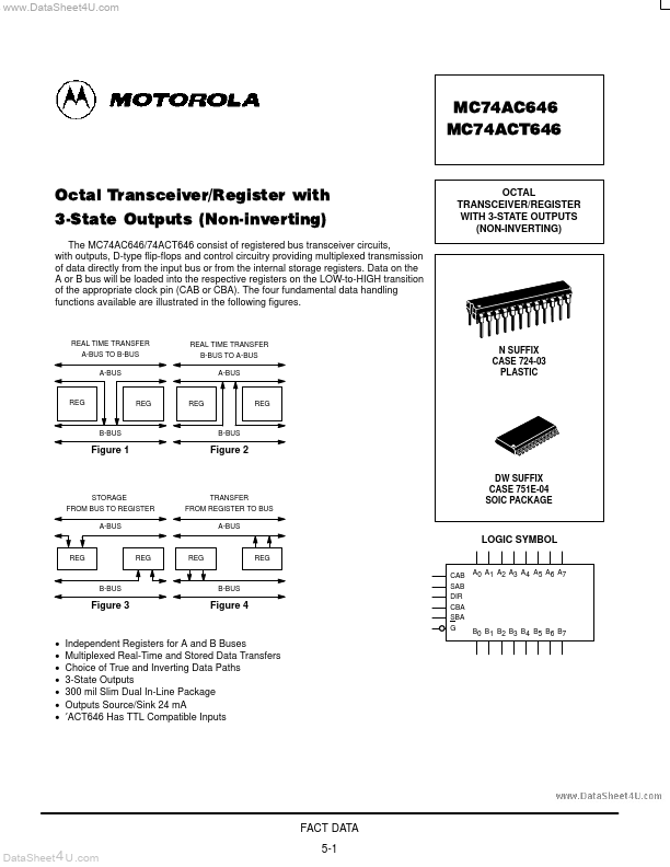
Independent Registers for A and B Buses Multiplexed Real-Time and Stored Data Transfers Choice of True and Inverting Data Paths 3-State Outputs 300 mil Slim Dual In-Line Package Outputs Source/Sink 24 m A ′ACT646 Has TTL patible Inputs FACT DATA Data Sheet 4 U . 5-1 .. MC74AC646 MC74ACT646 FUNCTION TABLE Inputs G H H L L L L DIR X X L L H H CAB H or L X X X H or L CBA H or L X X X X SAB X X X X L H SBA X X L H X X A0- A7 Input Output Input Data I/O- Operation or Function B0- B7 Input Input Output Isolation Store A and B Data Real Time B Data to A Bus Stored B Data to A Bus Real Time A Data to B Bus Stored A Data to B Bus - The data output functions may be enabled or disabled by various signals at the G and DIR inputs. Data input functions are always enabled; i.e., data at the bus pins will be stored on every LOW-to-HIGH transition of the appropriate clock inputs. H = HIGH Voltage Level L = LOW Voltage Level X = Immaterial =...