MC74F112
MC74F112 is DUAL JK NEGATIVE EDGE-TRIGGERED FLIP-FLOP manufactured by Motorola Semiconductor.
MC74F112 DUAL JK NEGATIVE EDGE-TRIGGERED FLIP-FLOP
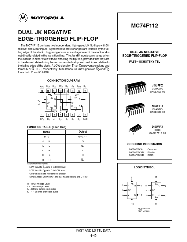
The MC74F112 contains two independent, high-speed JK flip-flops with Direct Set and Clear inputs. Synchronous state changes are initiated by the falling edge of the clock. Triggering occurs at a voltage level of the clock and is not directly related to the transition time. The J and K inputs can change when the clock is in either state without affecting the flip-flop, provided that they are in the desired state during the remended setup and hold times relative to the falling edge of the clock. A LOW signal on SD or CD prevents clocking and forces Q or Q HIGH, respectively. Simultaneous LOW signals on SD and CD force both Q and Q HIGH. CONNECTION DIAGRAM
VCC CD1 CD2 CP2 16 15 14 13 K2 12 J2 11 SD2 10 Q2 9
16 1
DUAL JK NEGATIVE EDGE-TRIGGERED FLIP-FLOP
FAST™ SCHOTTKY TTL
J SUFFIX CERAMIC CASE 620-09
C K D Q CP Q J SD 1 CP1 2 K1 3 J1 4 SD1 5 Q1
S J D Q CP K Q CD 6 Q1 7 Q2 8 GND
N SUFFIX PLASTIC CASE 648-08
FUNCTION TABLE (Each Half)
Inputs @ tn J L L H H
Asynchronous Inputs: LOW Input to SD sets Q to HIGH level LOW Input to CD sets Q to LOW level Clear and Set are independent of clock Simultaneous LOW on CD and SD makes both Q and Q HIGH H = HIGH Voltage Level L = LOW Voltage Level tn = Bit time before clock pulse tn + 1 = Bit time after clock pulse
Output @ tn + 1 Q Qn L H Qn
16 1
D SUFFIX SOIC CASE 751B-03
K L H L H
ORDERING INFORMATION
MC74FXXXJ MC74FXXXN MC74FXXXD Ceramic Plastic SOIC
LOGIC SYMBOL
4 3 1 2 J SD J
10 SD
11 13
CP K Q 6
CP K CD 14 Q 7
15 VCC = PIN 16 GND = PIN 8
FAST AND LS TTL DATA 4-45
LOGIC DIAGRAM (one half shown)
CD J CP
SD K
GUARANTEED OPERATING RANGES
Symbol VCC TA IOH IOL Supply Voltage Operating Ambient Temperature Range Output Current
- High Output...