MC74HC373A
MC74HC373A is Octal 3-State Non-Inverting Transparent Latch manufactured by Motorola Semiconductor.
MOTOROLA
SEMICONDUCTOR TECHNICAL DATA
Octal 3-State Non-Inverting Transparent Latch
High- Performance Silicon- Gate CMOS
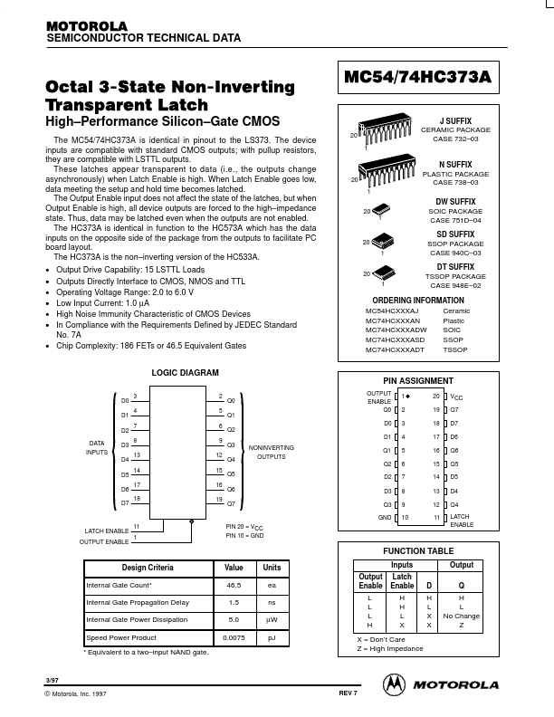
The MC54/74HC373A is identical in pinout to the LS373. The device inputs are patible with standard CMOS outputs; with pullup resistors, they are patible with LSTTL outputs. These latches appear transparent to data (i.e., the outputs change asynchronously) when Latch Enable is high. When Latch Enable goes low, data meeting the setup and hold time bees latched. The Output Enable input does not affect the state of the latches, but when Output Enable is high, all device outputs are forced to the high- impedance state. Thus, data may be latched even when the outputs are not enabled. The HC373A is identical in function to the HC573A which has the data inputs on the opposite side of the package from the outputs to facilitate PC board layout. The HC373A is the non- inverting version of the HC533A.
- -
- -
- - Output Drive Capability: 15 LSTTL Loads Outputs Directly Interface to CMOS, NMOS and TTL Operating Voltage Range: 2.0 to 6.0 V Low Input Current: 1.0 µA High Noise Immunity Characteristic of CMOS Devices In pliance with the Requirements Defined by JEDEC Standard No. 7A
- Chip plexity: 186 FETs or 46.5 Equivalent Gates LOGIC DIAGRAM
D0 D1 D2 DATA INPUTS D3 D4 D5 D6 D7 3 4 7 8 13 14 17 18 2 5 6 9 12 15 16 19 Q0 Q1 Q2
MC54/74HC373A
J SUFFIX CERAMIC PACKAGE CASE 732- 03
20 1 20 1
N SUFFIX PLASTIC PACKAGE CASE 738- 03 DW SUFFIX SOIC PACKAGE CASE 751D- 04 SD SUFFIX SSOP PACKAGE CASE 940C- 03 DT SUFFIX TSSOP PACKAGE CASE 948E- 02
20 1 20 1
ORDERING INFORMATION Ceramic MC54HCXXXAJ Plastic MC74HCXXXAN SOIC MC74HCXXXADW SSOP MC74HCXXXASD TSSOP MC74HCXXXADT
PIN ASSIGNMENT
OUTPUT ENABLE Q0 D0 D1 Q3 Q4 Q5 Q6 Q7 PIN 20 = VCC PIN 10 = GND NONINVERTING OUTPUTS Q1 Q2 D2 D3 Q3 GND 1 2 3 4 5 6 7 8 9 10 20 19 18 17 16 15 14 13 12 11 VCC Q7 D7 D6 Q6 Q5 D5 D4 Q4 LATCH ENABLE
LATCH ENABLE OUTPUT ENABLE
11 1
ÎÎÎÎÎÎÎÎÎÎ ÎÎÎÎ ÎÎÎ ÎÎÎÎÎÎÎÎÎÎ ÎÎÎÎ ÎÎÎ ÎÎÎÎÎÎÎÎÎÎ ÎÎÎÎ...