MC74HC646
MC74HC646 is Octal 3-State Bus Transeceivers and D Flip-Flops manufactured by Motorola Semiconductor.
MOTOROLA
SEMICONDUCTOR TECHNICAL DATA
Octal 3-State Bus Transceivers and D Flip-Flops
High- Performance Silicon- Gate CMOS
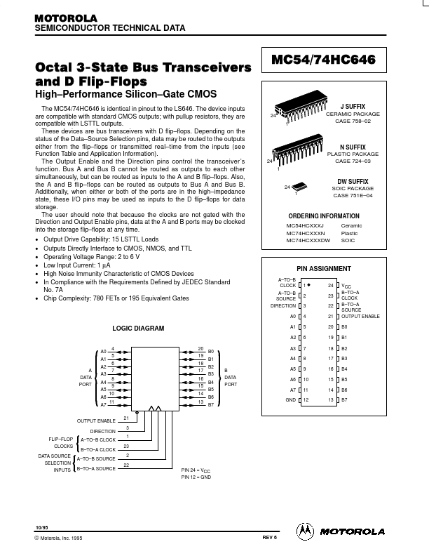
The MC54/74HC646 is identical in pinout to the LS646. The device inputs are patible with standard CMOS outputs; with pullup resistors, they are patible with LSTTL outputs. These devices are bus transceivers with D flip- flops. Depending on the status of the Data- Source Selection pins, data may be routed to the outputs either from the flip- flops or transmitted real- time from the inputs (see Function Table and Application Information). The Output Enable and the Direction pins control the transceiver’s function. Bus A and Bus B cannot be routed as outputs to each other simultaneously, but can be routed as inputs to the A and B flip- flops. Also, the A and B flip- flops can be routed as outputs to Bus A and Bus B. Additionally, when either or both of the ports are in the high- impedance state, these I/O pins may be used as inputs to the D flip- flops for data storage. The user should note that because the clocks are not gated with the Direction and Output Enable pins, data at the A and B ports may be clocked into the storage flip- flops at any time.
- -
- -
- - Output Drive Capability: 15 LSTTL Loads Outputs Directly Interface to CMOS, NMOS, and TTL Operating Voltage Range: 2 to 6 V Low Input Current: 1 µA High Noise Immunity Characteristic of CMOS Devices In pliance with the Requirements Defined by JEDEC Standard No. 7A
- Chip plexity: 780 FETs or 195 Equivalent Gates
MC54/74HC646
24 1
J SUFFIX CERAMIC PACKAGE CASE 758- 02
24 1
N SUFFIX PLASTIC PACKAGE CASE 724- 03
24 1
DW SUFFIX SOIC PACKAGE CASE 751E- 04
ORDERING INFORMATION MC54HCXXXJ MC74HCXXXN MC74HCXXXDW Ceramic Plastic SOIC
PIN ASSIGNMENT
A- TO- B CLOCK A- TO- B SOURCE DIRECTION A0 1 2 3 4 5 6 7 8 9 10 11 12 24 23 22 21 20 19 18 17 16 15 14 13 VCC B- TO- A CLOCK B- TO- A SOURCE OUTPUT ENABLE B0 B1 B2 B3 B4 B5 B6 B7
LOGIC DIAGRAM
4 5 6 7 8 9 10 11 21 3 1 23 2 22 PIN 24 = VCC PIN 12 = GND 20 19 18...