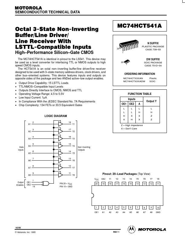
MC74HCT541A Description
MOTOROLA SEMICONDUCTOR TECHNICAL DATA Octal 3-State Non-Inverting Buffer/Line Driver/ Line Receiver With LSTTL-patible Inputs High Performance Silicon Gate CMOS The MC74HCT541A is identical in pinout to the LS541. This device may be used as a level converter for interfacing TTL or NMOS outputs to high speed CMOS inputs. The HCT541A is an octal non inverting buffer/line driver/line receiver designed to be used with 3...
MC74HCT541A Key Features
- Output Drive Capability: 15 LSTTL Loads TTL/NMOS-patible Input Levels Outputs Directly Interface to CMOS, NMOS and TTL O
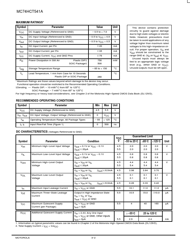
- 0.5 to + 7.0
- 0.5 to VCC + 0.5
- 0.5 to VCC + 0.5 ± 20 ± 35 ± 75 750 500 Vout Iin DC Output Voltage (Referenced to GND) DC Input Current, per Pin mA mA m
- 65 to + 150 260