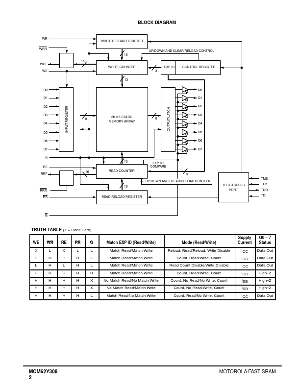
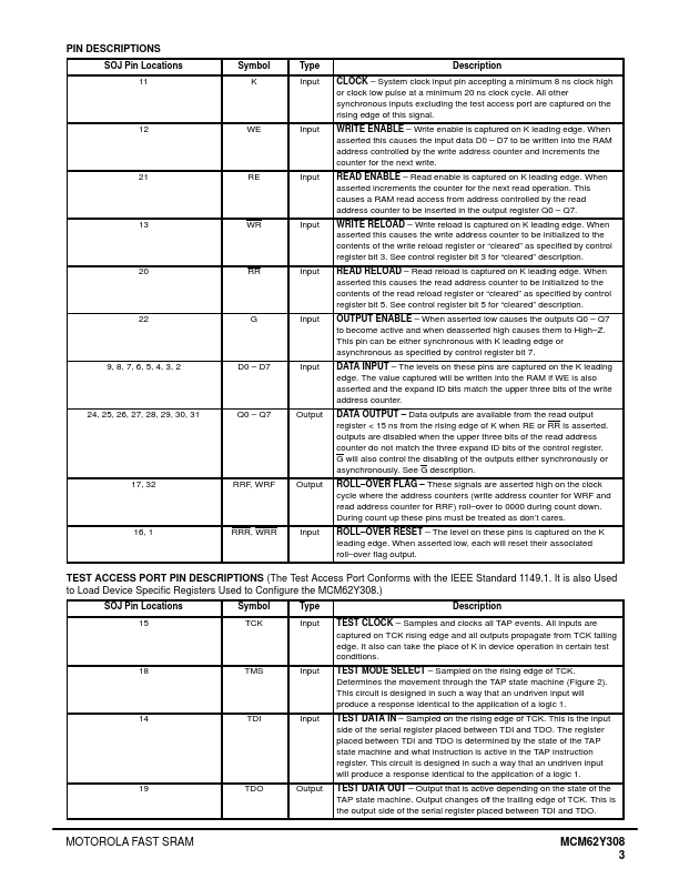
Datasheet4U Logo Datasheet4U.com

MCM62Y308 - Synchronous Line Buffer:8K x 8 Bit Fast Static Dual Ported Memory

General Description

SOJ Pin Locations 11 Symbol K Type Input Description CLOCK

System clock input pin accepting a minimum 8 ns clock high or clock low pulse at a minimum 20 ns clock cycle.

All other synchronous inputs excluding the test access port are captured on the rising edge of this signal.

Key Features

  • on the rising edge of TCK. This is the input side of the serial register placed between TDI and TDO. The register placed between TDI and TDO is determined by the state of the TAP state machine and what instruction is active in the TAP instruction register. This circuit is desig.

📥 Download Datasheet

Full PDF Text Transcription (Reference)

The following content is an automatically extracted verbatim text from the original manufacturer datasheet and is provided for reference purposes only.

View original datasheet text
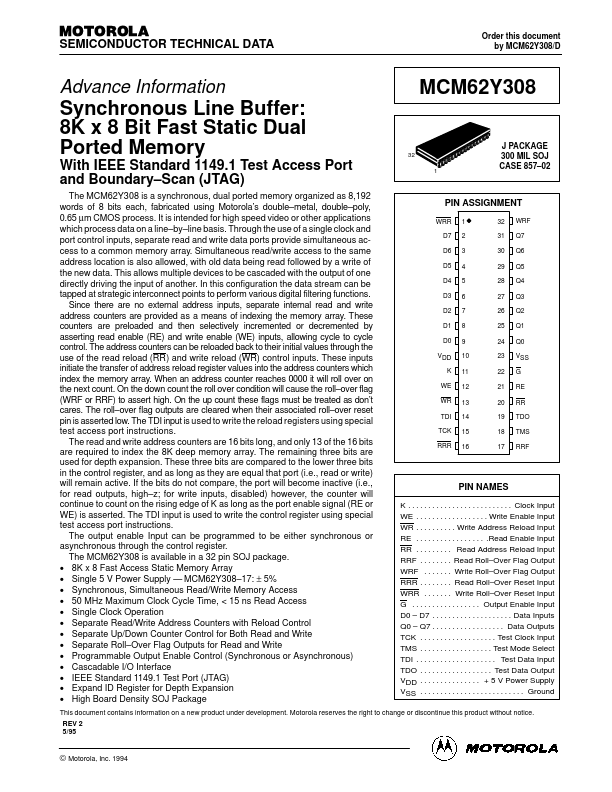
MOTOROLA SEMICONDUCTOR TECHNICAL DATA Order this document by MCM62Y308/D Advance Information MCM62Y308 J PACKAGE 300 MIL SOJ CASE 857–02 Synchronous Line Buffer: 8K x 8 Bit Fast Static Dual Ported Memory With IEEE Standard 1149.1 Test Access Port and Boundary–Scan (JTAG) The MCM62Y308 is a synchronous, dual ported memory organized as 8,192 words of 8 bits each, fabricated using Motorola’s double–metal, double–poly, 0.65 µm CMOS process. It is intended for high speed video or other applications which process data on a line–by–line basis. Through the use of a single clock and port control inputs, separate read and write data ports provide simultaneous access to a common memory array.