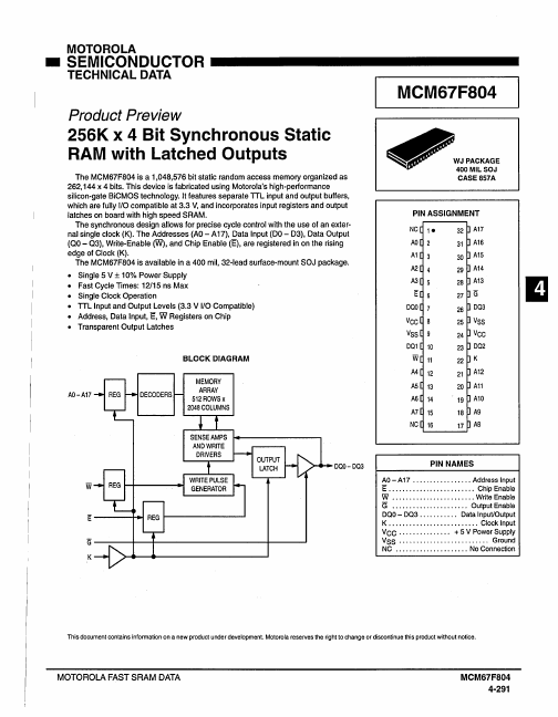
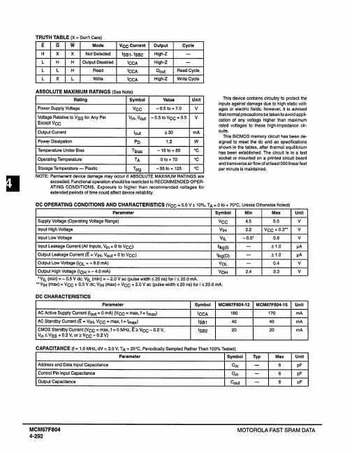
Datasheet4U Logo Datasheet4U.com

MCM67F804 - 256K x 4 Bit Synchronous Static RAM

Key Features

  • separate TTL input and output buffers, which are fully I/O compatible at 3.3 V, and incorporates input registers and output latches on board with high speed SRAM. The synchronous design allows for precise cycle control with the use of an external single clock (K). The Addresses (AO - A17), Data Input (DO - D3), Data Output (00 - 03), Write-Enable (W), and Chip Enable (E), are registered in on the rising edge of Clock (K). The MCM67F804 is available in a 400 mil, 32-lead surface-mount SOJ package.

📥 Download Datasheet

Full PDF Text Transcription (Reference)

The following content is an automatically extracted verbatim text from the original manufacturer datasheet and is provided for reference purposes only.

View original datasheet text
MOTOROLA • SEMICONDUCTOR TECHNICAL DATA Product Preview 256K x 4 Bit Synchronous Static RAM with Latched Outputs The MCM67F804 is a 1,048,576 bit static random access memory organized as 262,144 x 4 bits. This device is fabricated using Motorola's high-performance silicon-gate BiCMOS technology. It features separate TTL input and output buffers, which are fully I/O compatible at 3.3 V, and incorporates input registers and output latches on board with high speed SRAM. The synchronous design allows for precise cycle control with the use of an external single clock (K). The Addresses (AO - A17), Data Input (DO - D3), Data Output (00 - 03), Write-Enable (W), and Chip Enable (E), are registered in on the rising edge of Clock (K).