MCM67M618A
feature eliminates plex off- chip write pulse generation and provides increased flexibility for ining signals. Dual write enables (LW and UW) are provided to allow individually writeable bytes. LW controls DQ0
- DQ8 (the lower bits), while UW controls DQ9
- DQ17 (the upper bits). This device is ideally suited for systems that require wide data bus widths and cache memory.
- -
- -
- -
- -
- - Single 5 V ± 5% Power Supply Fast Access Times: 9/10/12 ns Max Byte Writeable via Dual Write Strobes Internal Input Registers (Address, Data, Control) Internally Self- Timed Write Cycle TSP, TSC, and BAA Burst Control Pins Asynchronous Output Enable Controlled Three- State Outputs mon Data Inputs and Data Outputs High Board Density 52- PLCC Package 3.3 V I/O patible
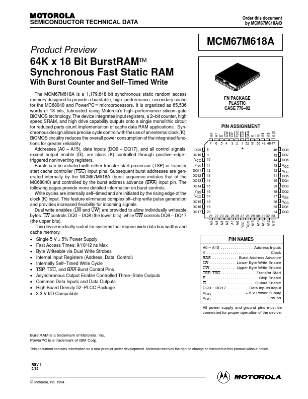
FN PACKAGE PLASTIC CASE 778- 02
PIN ASSIGNMENT
A6 A7 E UW LW TSC TSP BAA K G A8 A9 A10 DQ9 DQ10 VCC VSS DQ11 DQ12 DQ13 DQ14 VSS VCC DQ15 DQ16 DQ17 7 6 5 4 3 2 1 52 51 50 49 48 47 8 46 9 45 10 44 11 43 12 42 13 41 14 40 15 39 16 38 17 37 18...