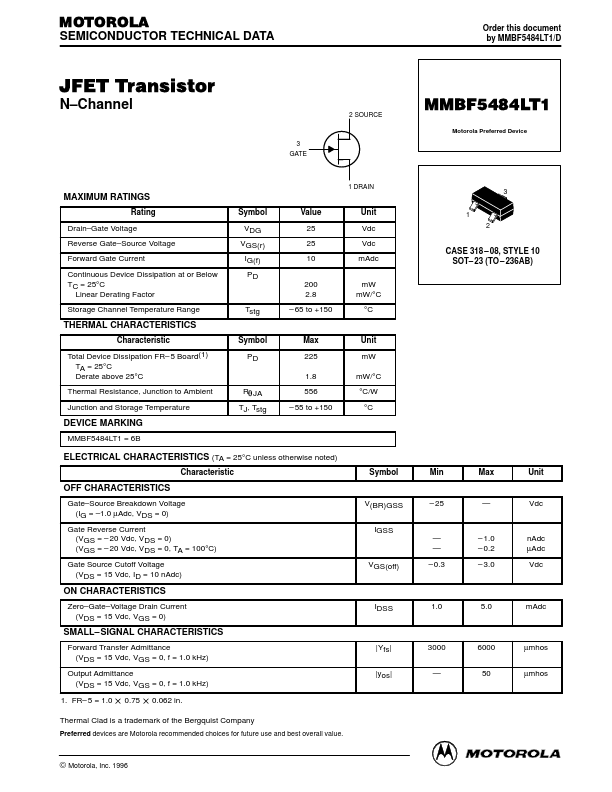
MMBF5484LT1 Overview
Key Features
- Gate Voltage Reverse Gate
- Source Voltage Forward Gate Current Continuous Device Dissipation at or Below TC = 25°C Linear Derating Factor Storage Channel Temperature Range Symbol VDG VGS(r) IG(f) PD 200 2.8 Tstg
| Part | MMBF5484LT1 |
|---|---|
| Description | JFET Transistor |
| Category | Transistor |
| Manufacturer | Motorola Semiconductor |
| Size | 294.72 KB |
| Part Number | Manufacturer | Description |
|---|---|---|
| MMBF5484 | onsemi | N-Channel RF Amplifier |
| MMBF5484 | Fairchild Semiconductor | N-Channel RF Amplifier |