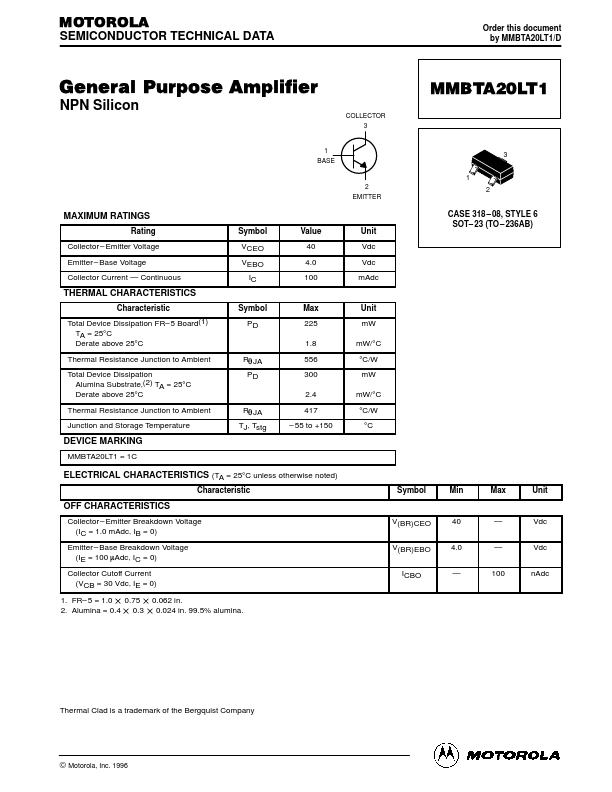
Datasheet4U Logo Datasheet4U.com

MMBTA20LT1 - General Purpose Amplifier

Key Features

  • n of the SOT.
  • 23 is a function of the pad size. This can vary from the minimum pad size for soldering to a pad size given for maximum power dissipation. Power dissipation for a surface mount device is determined by T J(max), the maximum rated junction temperature of the die,.

📥 Download Datasheet

Full PDF Text Transcription (Reference)

The following content is an automatically extracted verbatim text from the original manufacturer datasheet and is provided for reference purposes only.

View original datasheet text
MOTOROLA SEMICONDUCTOR TECHNICAL DATA Order this document by MMBTA20LT1/D General Purpose Amplifier NPN Silicon COLLECTOR 3 1 BASE MMBTA20LT1 3 1 2 EMITTER 2 MAXIMUM RATINGS Rating Collector – Emitter Voltage Emitter – Base Voltage Collector Current — Continuous Symbol VCEO VEBO IC Value 40 4.0 100 Unit Vdc Vdc mAdc CASE 318 – 08, STYLE 6 SOT– 23 (TO – 236AB) THERMAL CHARACTERISTICS Characteristic Total Device Dissipation FR– 5 Board(1) TA = 25°C Derate above 25°C Thermal Resistance Junction to Ambient Total Device Dissipation Alumina Substrate,(2) TA = 25°C Derate above 25°C Thermal Resistance Junction to Ambient Junction and Storage Temperature Symbol PD Max 225 1.8 RqJA PD 556 300 2.