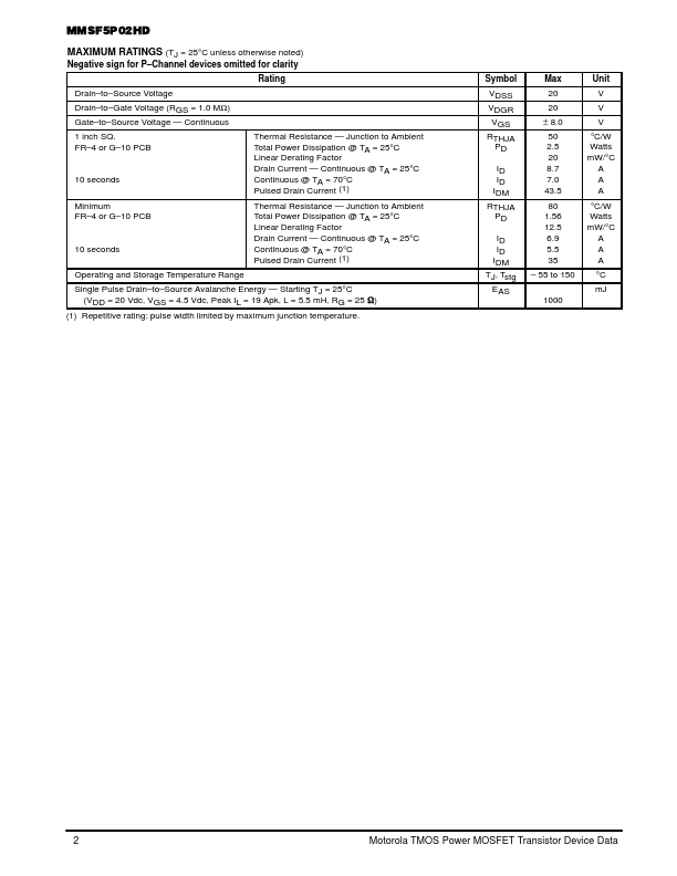
Motorola MMSF5P02HD
SINGLE TMOS POWER MOSFET
| Part No. | MMSF5P02HD |
|---|---|
| Datasheet | MMSF5P02HD Download |
| Manufacturer |  Motorola |
| Description | SINGLE TMOS POWER MOSFET |
| Buy | Stock & Price |
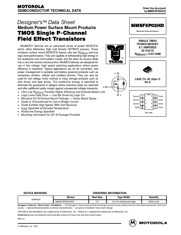
MAXIMUM RATINGS
(TJ = 25°C unless otherwise noted) Negative sign for P–Channel devices omitted for clarity Rating Drain–to–Source Voltage Drain–to–Gate Voltage (RGS = 1.0 MΩ) Gate–to–Source Voltage — Continuous 1 inch SQ. FR–4 or G–10 PCB Thermal Resistance — Junction to Ambient Total Power Dissipation @ TA = 25°C Linear Derating Factor Drain Current — Continuous @ TA = 25°C Continuous @ TA = 70°C Pulsed Drain Current (1) Thermal Resistance — Junction to Ambient Total Power Dissipation @ TA = 25°C Linear Derating Factor Drain Current — Continuous @ TA = 25°C Continuous @ TA = 70°C Pulsed Drain Current (1) Symbol VDSS VDGR VGS RTHJA PD ID ID IDM RTHJA PD ID ID IDM TJ, Tstg EAS 1000 Max 20 20 ± 8.0 50 2.5 20 8.7 7.0 43.5 80 1.56 12.5 6.9 5.5 35 – 55 to 150 Unit V V V °C/W Watts mW/°C A A A °C/W Watts mW/°C A A A °C mJ 10 seconds Minimum FR–4 or G–10 PCB 10 seconds Operating and Storage Temperature Range Single Pulse Drain–to–Source Avalanche Energy — Starting TJ = 25°C (VDD = 20 Vdc, VGS = 4.5 Vdc, Peak IL = 19 Apk, L = 5.5 mH, RG = 25 W) (1) Repetitive rating; pulse width limited by maximum junction temperature.