Datasheet4U Logo Datasheet4U.com

MPC9100 - DUAL PLL CLOCK GENERATOR

General Description

Pin Q_31 Q_14 Q_45 VCCO_XX GNDO_XX VCCI GNDI VCCAX GNDAX XTAL1 XTAL2 TCLK FCAPXX FCAPXXP Description 31.3344MHz Output 14.318MHz Output 45.1584MHz Output Output Buffer Power Supply Output Buffer Ground Core Logic Power Supply Core Logic Ground PLL Power Supply PLL Ground Crystal Oscillator Input Cry

Key Features

  • a fully integrated crystal oscillator as the clock reference source. No external components are required other than the 14.318 MHz crystal. The TCLK input is used only for factory test and cannot be used as the PLL clock reference. To reduce total die area the PLL loop filter capacitors are brought outside the chip. The FCAP pins are used to connect these capacitors to the internal PLL’s. 0.01µf capacitors www. DataSheet4U. com are recommended. The device features three synchronous output enable p.

📥 Download Datasheet

Full PDF Text Transcription (Reference)

The following content is an automatically extracted verbatim text from the original manufacturer datasheet and is provided for reference purposes only.

View original datasheet text
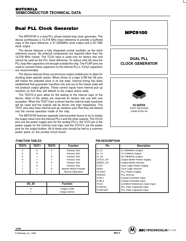
MOTOROLA SEMICONDUCTOR TECHNICAL DATA Dual PLL Clock Generator The MPC9100 is a dual PLL phase locked loop clock generator. The device synthesizes a 14.318 MHz input reference to provide a buffered copy of the input reference, a 31.3344MHz clock output and a 45.1584 clock output. The device features a fully integrated crystal oscillator as the clock reference source. No external components are required other than the 14.318 MHz crystal. The TCLK input is used only for factory test and cannot be used as the PLL clock reference. To reduce total die area the PLL loop filter capacitors are brought outside the chip. The FCAP pins are used to connect these capacitors to the internal PLL’s. 0.01µf capacitors www.DataSheet4U.com are recommended.