Datasheet4U Logo Datasheet4U.com

MPC949 - 
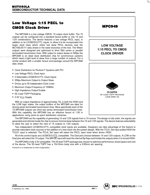
LOW VOLTAGE 1:15 PECL TO CMOS CLOCK DRIVER

General Description

Pin Name TCLK_Sel (Int Pulldown) TCLK0:1 (Int Pullup) PCLK (Int Pulldown) PCLK (Int Pullup) Dseln (Int Pulldown) MR/OE (Int Pulldown) PCLK_Sel (Int Pulldown) Function Select pin to choose TCKL0 or TCLK1 LVCMOS/LVTTL clock inputs True PECL clock input Compliment PECL clock input 1x or 1/2x input divi

Key Features

  • a low voltage PECL input, in addition to its LVCMOS/LVTTL inputs, to allow it to be incorporated into larger clock trees which utilize low skew PECL devices (see the MC100LVE111 data sheet) in the lower branches of the tree. The fifteen outputs were designed and optimized to drive 50Ω series or parallel terminated transmission lines. With output to output skews of 300ps the MPC949 is an ideal clock distribution chip for synchronous systems www. DataSheet4U. com which need a tight level of skew fro.

📥 Download Datasheet

Full PDF Text Transcription (Reference)

The following content is an automatically extracted verbatim text from the original manufacturer datasheet and is provided for reference purposes only.

View original datasheet text
MOTOROLA SEMICONDUCTOR TECHNICAL DATA Low Voltage 1:15 PECL to CMOS Clock Driver The MPC949 is a low voltage CMOS, 15 output clock buffer. The 15 outputs can be configured into a standard fanout buffer or into 1X and 1/2X combinations. The device features a low voltage PECL input, in addition to its LVCMOS/LVTTL inputs, to allow it to be incorporated into larger clock trees which utilize low skew PECL devices (see the MC100LVE111 data sheet) in the lower branches of the tree. The fifteen outputs were designed and optimized to drive 50Ω series or parallel terminated transmission lines. With output to output skews of 300ps the MPC949 is an ideal clock distribution chip for synchronous systems www.DataSheet4U.com which need a tight level of skew from a large number of outputs.