Datasheet4U.com
🌙
MPC952 Datasheet | Motorola Semiconductor
Part:
MPC952
Description:
LOW VOLTAGE PLL CLOCK DRIVER
Manufacturer:
Motorola Semiconductor
Size:
108.87 KB
MPC952 Datasheet (PDF) Download
Related MPC952 Datasheets
MPC953 LOW VOLTAGE PLL CLOCK DRIVER
MPC950 LOW VOLTAGE PLL CLOCK DRIVER
MPC954 LOW VOLTAGE PLL CLOCK DRIVER
MPC958 LOW VOLTAGE PLL CLOCK DRIVER
MPC951 LOW VOLTAGE PLL CLOCK DRIVER
Motorola Semiconductor
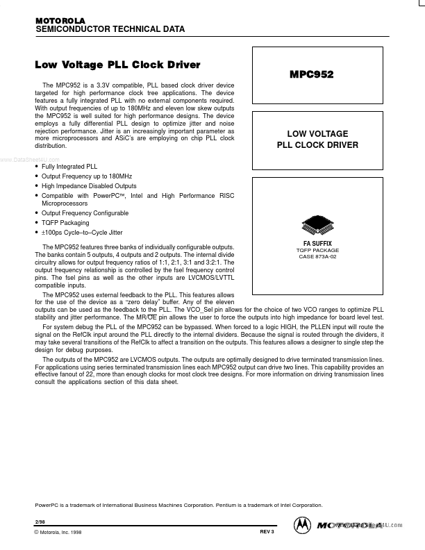
MPC952
Key Features
Output Frequency Configurable
TQFP Packaging
±100ps Cycle–to–Cycle Jitter
MPC952 Logic Diagram
32–Lead Pinout (Top View)
×
Close