MPF910
MOTOROLA
SEMICONDUCTOR TECHNICAL DATA
TMOS Switching
N- Channel
- Enhancement
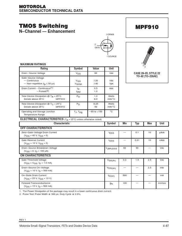
3 DRAIN
2 GATE
1 SOURCE
MAXIMUM RATINGS Rating
Symbol
Value
Unit
Drain
- Source Voltage
Gate- Source Voltage
- Continuous
- Non- repetitive (tp ≤ 50 µs)
Drain Current
- Continuous(1)
- Pulsed(2)
Total Device Dissipation @ TA = 25°C
Derate above 25°C
VGS VGSM
ID IDM PD
60 Vdc
± 20 Vdc ± 40 Vpk 0.5 Adc 1.0
1.0 Watts 8.0 m W/°C
Total Device Dissipation @ TC = 25°C
Derate above 25°C
MFE910
6.25 Watts 50 m W/°C
Operating and Storage Junction Temperature Range
TJ, Tstg
- 65 to +150
°C
ELECTRICAL CHARACTERISTICS (TA = 25°C unless otherwise noted) Characteristic
Symbol
OFF CHARACTERISTICS
Zero- Gate- Voltage Drain Current (VDS = 40 V, VGS =...