MPF970
MPF970 MPF971
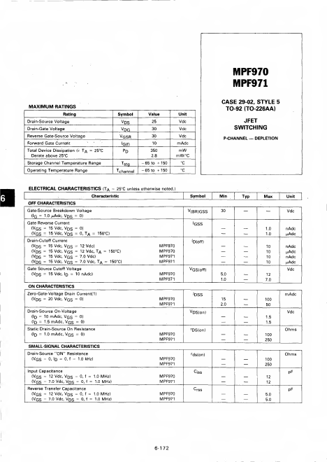
MAXIMUM RATINGS
Rating Drain-Source Voltage Drain-Gate Voltage Reverse Gate-Source Voltage Forward Gate Current
Total Device Dissipation (a TA = 25°C
Derate above 25°C Storage Channel Temperature Range Operating Temperature Range
Symbol v Ds v Dg vgsr
'G(f)
T stq ^channel
Value 25 30 30 10 350 2.8
-65 to +150 -65 to +150
Unit Vdc Vdc Vdc m Adc m W m W/°C
°C
°C
CASE 29-02, STYLE 5
TO-92 (TO-226AA)
JFET SWITCHING
- P-CHANNEL DEPLETION
ELECTRICAL CHARACTERISTICS (TA = 25°C unless otherwise noted.
Characteristic
OFF CHARACTERISTICS
Gate-Source Breakdown Voltage G(l = 1.0/i Adc, V DS = 0)
Gate Reverse Current
(V GS = 15 Vdc, V DS = 0) (V GS = 15 Vdc, V DS = 0, TA = 150°C)
Drain-Cutoff Current
(Vq S = 15 Vdc, Vqs = 12 Vdc) (V D s = 15 Vdc, Vqs = 12 Vdc, TA = 150°C) (Vps = 15 Vdc, Vqs = 7.0 Vdc) (Vd S = 15 Vdc, V G S = 7.0 Vdc, TA = 150°C)
Gate Source Cutoff Voltage (VD s = 15 Vdc, Id = 10 n Adc)
ON CHARACTERISTICS
MPF970 MPF970 MPF971 MPF971
MPF970 MPF971
Zero-Gat...