Datasheet4U.com
🌙
MPQ6427 Datasheet | Motorola Semiconductor
Part:
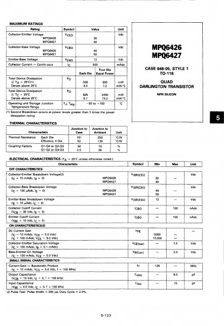
MPQ6427
Description:
QUAD DARLINGTON TRANSISTOR
Category:
Transistor
Manufacturer:
Motorola Semiconductor
Size:
83.22 KB
MPQ6427 Datasheet (PDF) Download
Related MPQ6427 Datasheets
MPQ6426 Quad Darlington Transistor
Motorola Semiconductor
MPQ6427
Key Features
55 to + 1 50
Datasheets by Manufacturer
Part Number
Manufacturer
Description
MPQ6427
National Semiconductor
NPN Darlington Transistor
×
Close