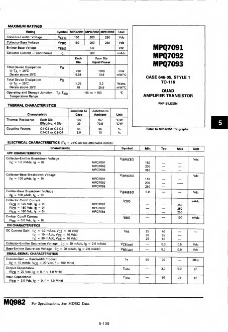
Full PDF Text Transcription for MPQ7092 (Reference)
Note: Below is a high-fidelity text extraction (approx. 800 characters) for
MPQ7092. For precise diagrams, and layout, please refer to the original PDF.
MAXIMUM RATINGS Rating Collector-Emitter Voltage Collector-Base Voltage Emitter-Base Voltage —Collector Current Continuous Total Device Dissipation @ TA = 25°C Derate abo...
View more extracted text
tor Current Continuous Total Device Dissipation @ TA = 25°C Derate above 25°C Total Device Dissipation @ Tc = 25°C Derate above 25°C Operating and Storage Junction Temperature Range Symbol MPQ7091 MPQ7092 MPQ7093 Unit VCEO 150 200 250 Vdc vCBO 150 200 250 Vdc VE BO 5.0 Vdc ic 500 mAdc Each Die Four Die Equal Power PD . 750 5.98 1700 13.6 mW mW/°C pd TJ' Tstg 1.25 10 3.2 25.6 - 55 to + 1 50 Watts mW/°C °C THERMAL CHARACTERISTICS Characteristic Thermal Resistance Each Die Effective, 4 Die Coupling Factors Q1-Q4 or Q2-Q3 Q1-Q2orQ3-Q4 Junction to Case 100 39 46 5.0 Junction to Ambient 167 73.
More Datasheets from Motorola Semiconductor (now NXP Semiconductors)