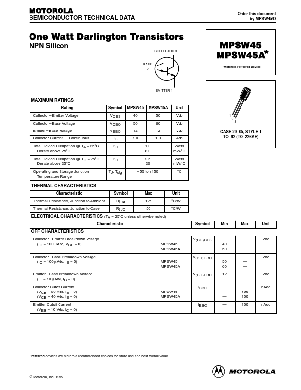
MPSW45 Datasheet Text
MOTOROLA
SEMICONDUCTOR TECHNICAL DATA
Order this document by MPSW45/D
One Watt Darlington Transistors
NPN Silicon
COLLECTOR 3 BASE 2
MPSW45 MPSW45A-
- Motorola Preferred Device
EMITTER 1
MAXIMUM RATINGS
Rating Collector
- Emitter Voltage Collector
- Base Voltage Emitter
- Base Voltage Collector Current
- Continuous Total Device Dissipation @ TA = 25°C Derate above 25°C Total Device Dissipation @ TC = 25°C Derate above 25°C Operating and Storage Junction Temperature Range Symbol VCES VCBO VEBO IC PD PD TJ, Tstg MPSW45 40 50 12 1.0 1.0 8.0 2.5 20
- 55 to +150 MPSW45A 50 60 12 1.0 Unit Vdc Vdc Vdc Adc Watts mW/°C Watts mW/°C °C
1 2 3
CASE 29- 05, STYLE 1 TO- 92 (TO- 226AE)
THERMAL CHARACTERISTICS
Characteristic Thermal Resistance, Junction to Ambient Thermal Resistance, Junction to Case Symbol RqJA RqJC Max 125 50 Unit °C/W °C/W
ELECTRICAL CHARACTERISTICS (TA = 25°C unless otherwise noted)
Characteristic Symbol Min Max Unit
OFF CHARACTERISTICS
Collector
- Emitter Breakdown Voltage (IC = 100 µAdc, VBE = 0) Collector
- Base Breakdown Voltage (IC = 100 mAdc, IE = 0) Emitter
- Base Breakdown Voltage (IE = 10 mAdc, IC = 0) Collector Cutoff Current (VCB = 30 Vdc, IE = 0) (VCB = 40 Vdc, IE = 0) Emitter Cutoff Current (VEB = 10 Vdc, IC = 0) MPSW45 MPSW45A IEBO V(BR)CES MPSW45 MPSW45A V(BR)CBO MPSW45 MPSW45A V(BR)EBO ICBO
- -
- 100 100 100 nAdc 50 60 12
- - ...