MRFIC1859
Key Features
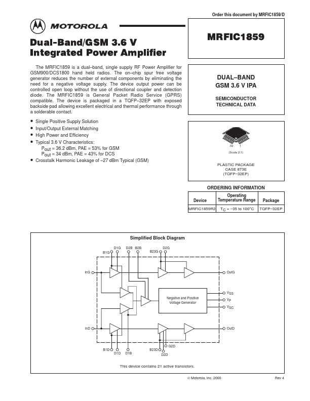
- Single Positive Supply Solution Input/Output External Matching High Power and Efficiency Typical 3.6 V Characteristics: Pout = 36.2 dBm, PAE = 53% for GSM Pout = 34 dBm, PAE = 43% for DCS Crosstalk Harmonic Leakage of –27 dBm Typical (GSM)