MSD6150
MSD6150 is Dual Diode Common Anode manufactured by Motorola Semiconductor.
MOTOROLA
SEMICONDUCTOR TECHNICAL DATA
Order this document by MSD6150/D
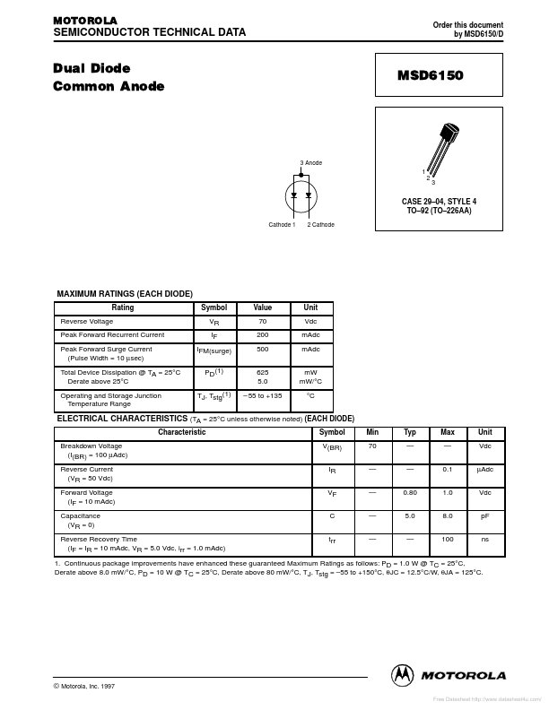
Dual Diode mon Anode
3 Anode
1 2 3
CASE 29- 04, STYLE 4 TO- 92 (TO- 226AA) Cathode 1 2 Cathode
MAXIMUM RATINGS (EACH DIODE)
Rating Reverse Voltage Peak Forward Recurrent Current Peak Forward Surge Current (Pulse Width = 10 µsec) Total Device Dissipation @ TA = 25°C Derate above 25°C Operating and Storage Junction Temperature Range Symbol VR IF IFM(surge) PD(1) TJ, Tstg(1) Value 70 200 500 625 5.0
- 55 to +135 Unit Vdc mAdc mAdc mW mW/°C °C
ELECTRICAL CHARACTERISTICS (TA = 25°C unless otherwise noted) (EACH DIODE)
Characteristic Breakdown Voltage (I(BR) = 100 µAdc) Reverse Current (VR = 50 Vdc) Forward...