Datasheet4U.com
🌙
MTP30P06V Datasheet | Motorola Semiconductor
Part:
MTP30P06V
Description:
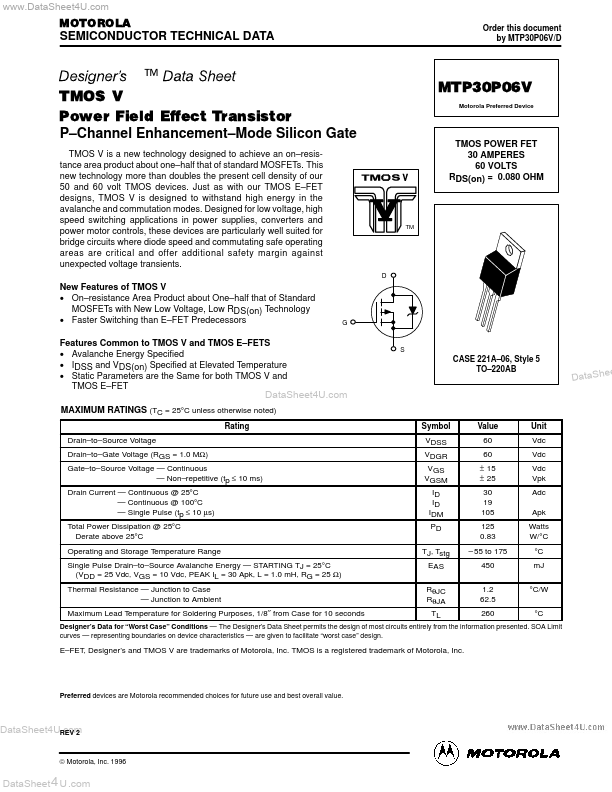
TMOS POWER FET 30 AMPERES 60 VOLTS RDS(on) = 0.080 OHM
Manufacturer:
Motorola Semiconductor
Size:
325.35 KB
MTP30P06V Datasheet (PDF) Download
Motorola Semiconductor
MTP30P06V
Key Features
On–resistance Area Product about One–half that of Standard MOSFETs with New Low Voltage, Low RDS(on) Technology
Avalanche Energy Specified
IDSS and VDS(on) Specified at Elevated Temperature
×
Close